13-2 UHF1 Schematic Diagrams, Overlays, and Parts Lists: Introduction
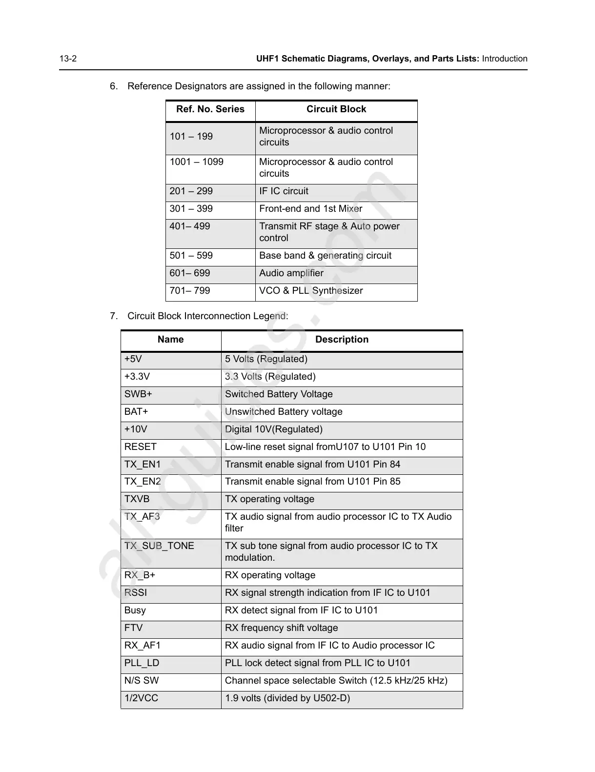
6. Reference Designators are assigned in the following manner:
7. Circuit Block Interconnection Legend:
Ref. No. Series Circuit Block
101 – 199
Microprocessor & audio control
circuits
1001 – 1099 Microprocessor & audio control
circuits
201 – 299 IF IC circuit
301 – 399 Front-end and 1st Mixer
401– 499 Transmit RF stage & Auto power
control
501 – 599 Base band & generating circuit
601– 699 Audio amplifier
701– 799 VCO & PLL Synthesizer
Name Description
+5V 5 Volts (Regulated)
+3.3V 3.3 Volts (Regulated)
SWB+ Switched Battery Voltage
BAT+ Unswitched Battery voltage
+10V Digital 10V(Regulated)
RESET Low-line reset signal fromU107 to U101 Pin 10
TX_EN1 Transmit enable signal from U101 Pin 84
TX_EN2 Transmit enable signal from U101 Pin 85
TXVB TX operating voltage
TX_AF3 TX audio signal from audio processor IC to TX Audio
filter
TX_SUB_TONE TX sub tone signal from audio processor IC to TX
modulation.
RX_B+ RX operating voltage
RSSI RX signal strength indication from IF IC to U101
Busy RX detect signal from IF IC to U101
FTV RX frequency shift voltage
RX_AF1 RX audio signal from IF IC to Audio processor IC
PLL_LD PLL lock detect signal from PLL IC to U101
N/S SW Channel space selectable Switch (12.5 kHz/25 kHz)
1/2VCC 1.9 volts (divided by U502-D)

 Loading...