Frequency Generation Circuit 2-9
In addition to the VCO, the synthesizer must interface with the logic and ASFIC circuitry.
Programming for the synthesizer is accomplished through the data, clock and chip select lines (pins
7, 8 and 9) from the microprocessor, U409. A 3.3V dc signal from pin 4 indicates to the
microprocessor that the synthesizer is locked.
Transmit modulation from the ASFIC is supplied to pin10 of U3701. Internally the audio is digitized
by the Fractional-N and applied to the loop divider to provide low-port modulation. The audio runs
through an internal attenuator for modulation balancing purposes before going out at pin 41 to the
VCO.
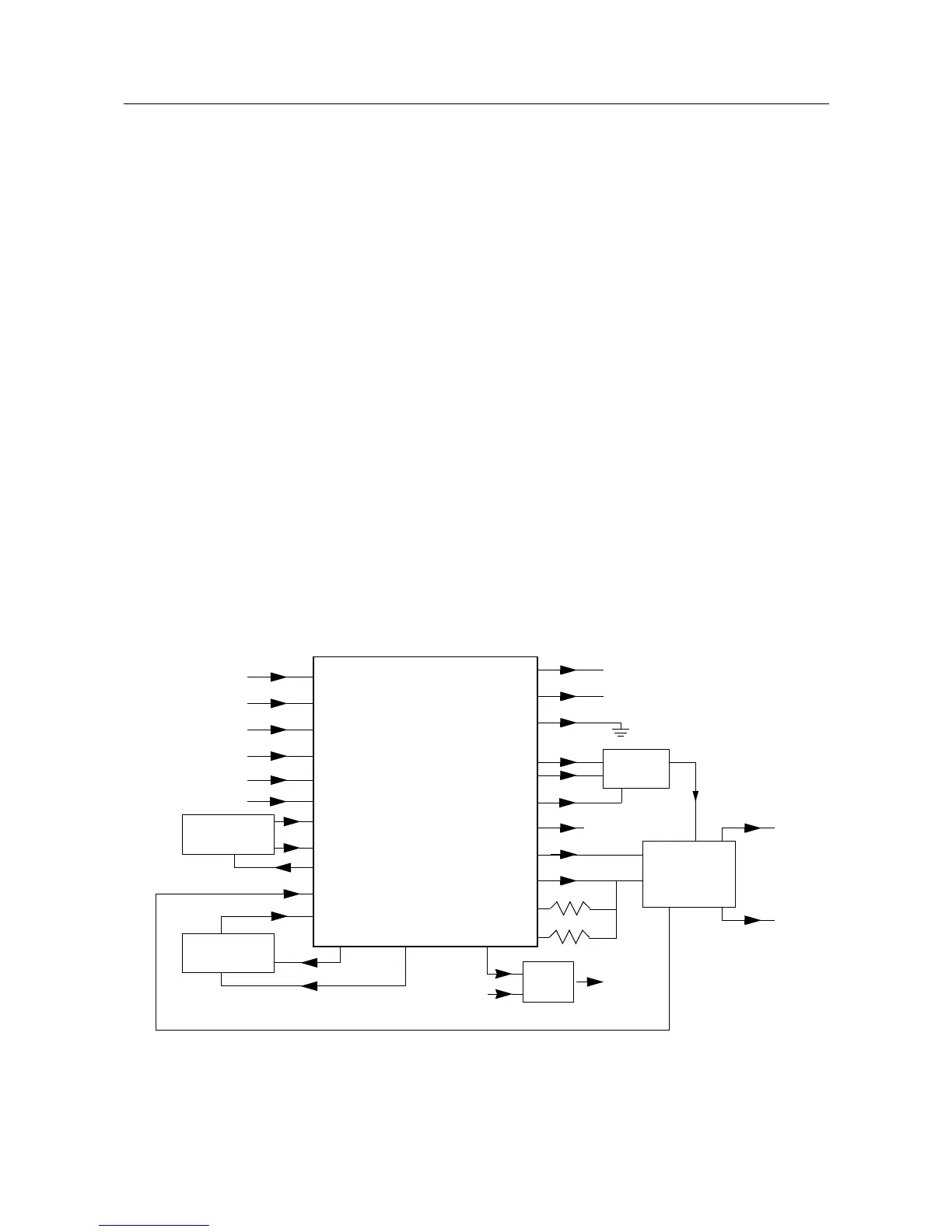
5.1 Synthesizer
The Fractional-N Synthesizer, shown in Figure 2-5, uses a 16.8MHz crystal (Y3761) to provide a
reference for the system. The LVFractN IC (U3701) further divides this to 2.1MHz, 2.225MHz, and
2.4MHz as reference frequencies. Together with C3761, C3762, C3763, R3761, and D3761, they
build up the reference oscillator that is capable of 2.5 ppm stability over temperatures of -30 to 85° C.
A 16.8MHz signal at pin 19 of U3701 is also provided for use by ASFIC and LVZIF (for all models
except those with PCB8486473Z04).
The loop filter which consist of C3721, C3722, R3721, R3722 and R3723 provides the necessary dc
steering voltage for the VCO and determines the amount of noise and spur passing through.
In achieving fast locking for the synthesizer, an internal adapt charge pump provides higher current
at pin 45 of U3701 to put the synthesizer within lock range. The required frequency is then locked by
normal mode charge pump at pin 43.
Both the normal and adapt charge pumps get their supply from the capacitive voltage multiplier
made up of C3701 to C3704 and triple diodes D3701, D3702. Two 3.3V square waves (180 degrees
out of phase) are first multiplied by four and then shifted, along with regulated 5V, to build up 13.5V
at pin 47 of U3701.
Figure 2-5 VHF Synthesizer Block Diagram.
DATA
CLK
CEX
MODIN
VCC, DC5V
XTAL1
XTAL2
WARP
PREIN
VCP
REFERENCE
OSCILLATOR
VOLTAGE
MULTIPLIER
VOLTAGE
CONTROLLED
OSCILLATOR
2-POLE
LOOP
FILTER
DATA (U409 PIN 100)
CLOCK (U409 PIN 1)
CSX (U409 PIN 2)
MOD IN (U404 PIN 40)
+5V (U3711 PIN 4)
7
8
9
10
13, 30
23
24
25
32
47
VMULT2 VMULT1
BIAS1
SFOUT
AUX3
AUX4
IADAPT
IOUT
GND
FREFOUT
LOCK
4
19
6, 22, 23, 24
43
45
3
2
28
14
15
40
FILTERED 5V
STEERING
LINE
LOCK (U409 PIN 56)
PRESCALER IN
LO RF INJECTION
TX RF INJECTION
(1ST STAGE OF PA
 Loading...