5
5
4
4
3
3
2
2
1
1
D D
C C
B B
A A
Title
Size Document Number Rev
Date: Sheet
of
MICRO-START INT'L CO.,LTD.
MS-7318-101-060918A 100
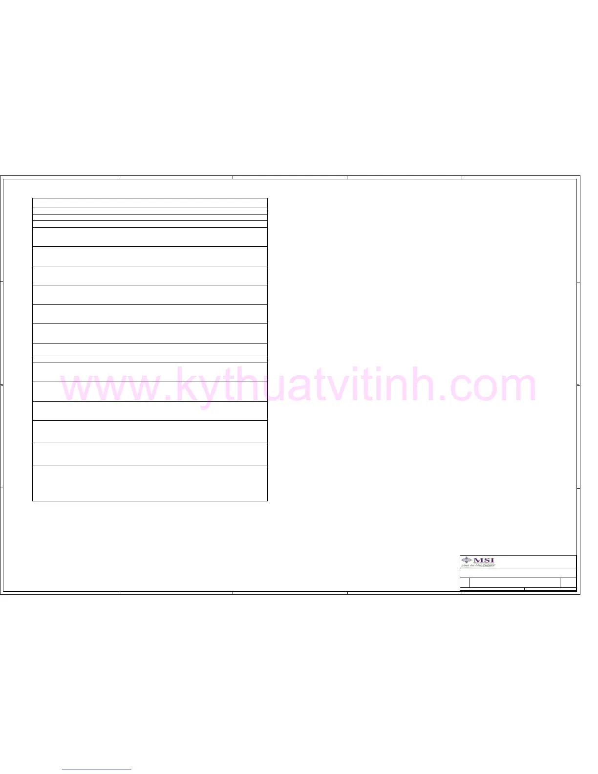
Strap Pins
445Monday, September 18, 2006
Title
Size Document Number Rev
Date: Sheet of
MICRO-START INT'L CO.,LTD.
MS-7318-101-060918A 100
Strap Pins
445Monday, September 18, 2006
Title
Size Document Number Rev
Date: Sheet of
MICRO-START INT'L CO.,LTD.
MS-7318-101-060918A 100
Strap Pins
445Monday, September 18, 2006
Pin#
ACSYNC LPC FWH
H: Disable Auto Reboot .
Default setting: Disable
ACSDOUT0
SEEDI B13 Use Serial L: Enable. Use external EEPROM
H: Disable. Do not use external EEPROM
R04
H: Disable LPC FWH Command
Auto Reboot
Signal Description
L: Enable CPU Frequency Strapping
H: Disable CPU Frequency Strapping
Default setting: Enable (pull low) sInc
L: Enable LPC FWH Command
SPKR
External LAN
AF05
Function
CPU Frequency
Strapping
EEPROM
Default setting: Disable
L: Enable Auto Reboot
SB-VT5251LCE
(External pullup / pulldown straps are required to select “H” / “L”)
Strap Pins for VT8251L Version CE Configuration
R01
Strap Pins
H: Disable SATA spin up mode
GPIOD /
PCGNTB
AC05 NB Configuration
H: Desktop LAN reset hnoideequ
Default setting: Disable
L: Enable SATA spin up mode iel SATA Spin
Up Mode
SUSA#
Mode
Strap Pins for North Bridge (“NB”) Configuration
Desktop LAN Reset
PDCS3# AA23 NB Configuration ATeCon PDCS3# signal state is reflected on
signal pin VD7 during power up for
North Bridge configuration.
GPIOB /
PCREQB
PDA2 signal state is reflected on
signal pin VD6 during power up for
North Bridge configuration.
AE01 GPIOB/PCREQB signal state is
reflected on signal pin VD2
during power up for North
Bridge configuration.
NB Configuration
Notebook /
AB23
Default setting: Disable
L: Enable PCI Express debugging mode logntiaired
H: Disable PCI Express debugging mode
PDA1 signal state is reflected on
signal pin VD5 during power up for
North Bridge configuration. DAR
NGPIOD/PCGNTB signal state is
reflected on signal pin VD3 during
power up for North Bridge
configuration.
PDDACK#
AD27 PDA2 NB Configuration
W01
Vlink auto compensation
PCI Express
Debugging
PDA1 AC26 NB Configuration
Default setting: Disable
L: Notebook LAN reset
PDCS1# AC25
NB Configuration
PDA0, AE03
AF03
PDA0, GPIOA/PCREQA and
GPIOC/PCGNTA signal states
are reflected on signal pins
VD4, VD1 and VD0 during
power up for North Bridge
configuration.
GPIOA/PCREQA
GPIOC/PCGNTA