Chapter 2 Theory of Operation
PCI E Series RLPM 2-20
©
National Instruments Corporation
Refer to the DAQ-STC Technical Reference Manual and the NI-DAQ
Function Reference Manual for more information on analog triggering.
For a detailed description of these modes, and timing diagrams, and for a
description of other modes not discussed here, refer to the DAQ-STC
Technical Reference Manual.
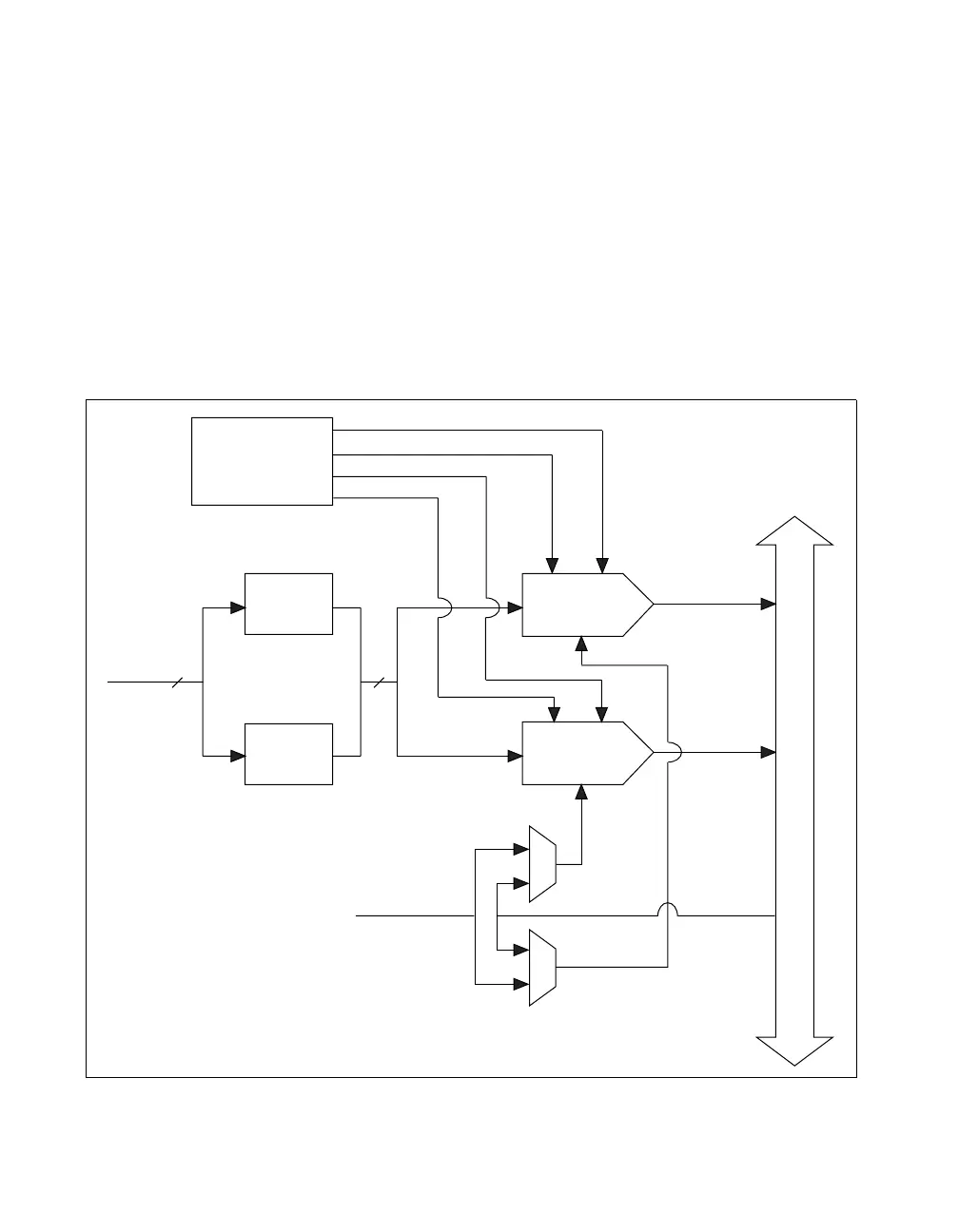
Analog Output and Timing Circuitry
The PCI E Series boards (except the PCI-6023E, PCI-6032E and
PCI-6033E) have two analog output channels and a timing core within the
DAQ-STC that is dedicated to analog output operation. Figure 2-17 shows
a general block diagram for the analog output circuitry.
Figure 2-17.
Analog Output Circuitry Block Diagram
DAQ-STC
I/O Connector
FIFO DAC0
DAC0OUT
DAC1OUT
Extref
DAC1
Data Bus
+10 V Reference
FIFO
Bypass
LDAC0*
DAC0WR*
LDAC1*
DAC1WR*
MUX
MUX
 Loading...