8 • Operation NEW FOCUS, Inc.
Theory
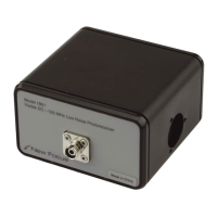
The Model 1801 photoreceiver contains a silicon/PIN
photodiode. The Model 1811 contains an InGaAs/PIN
photodiode. In both models, the photodiode is fol-
lowed by a low-noise transimpedance amplifier acting
as a pre-amp with a compensating amplifier as the out-
put stage. A functional block diagram of the DC-cou-
pled version is shown in Figure 1.
The AC-coupled versions incorporate two extra
blocking capacitors, a choke, and a DC bias monitor
circuit. The corner frequency of the high-pass filter on
the AC-coupled output is approximately 25 kHz. The
corner frequency of the low-pass filter on the DC bias
monitor output is approximately 50 kHz. Refer to
Figure 2 for a functional block diagram.
The compensating amplifier allows us to use a large-
area diode, which is intrinsically low speed, while
maintaining a large bandwidth with flat response. This
is accomplished by having the gain of the output stage
increase with frequency. As a result of the increasing
gain the noise floor of the receiver increases starting at
approx. 40 MHz and having a soft peak at approxi-
mately 110 MHz. The equivalent input noise current at
the peak is greater than the low-frequency noise by a
factor of 10. Typical frequency response and noise
floor is shown in Figure 5.
The transimpedance amplifier in the AC path has an
absolute maximum input current of 5 mA and
therefore the maximum input optical power is 7 mW.
Figure 3 and Figure 4 show the responsivity of the
photodiodes. Power is delivered through a connector
on the back of the unit and the entire package is
shielded to eliminate RF pickup.
18X1 HS rcvr rev G.fm Page 8 Thursday, September 20, 2001 2:08 PM
Artisan Scientific - Quality Instrumentation ... Guaranteed | (888) 88-SOURCE | www.artisan-scientific.com