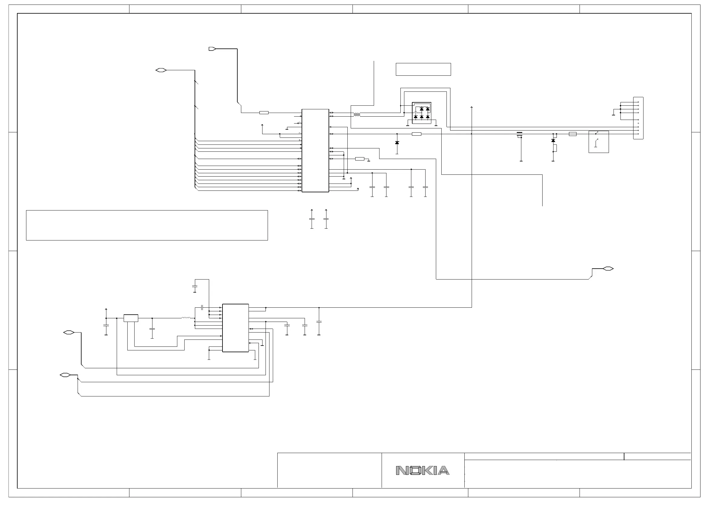
GAZOO LS A/D CONVERTER
VBUS PIN
The tolerance has to be 1%
Place R3304 as close to Rapu as possible
2
SDA
1
Pins E4 and E2 must be connected to the battery with separate wires
SCL
(this side of green barrier)
3
1
CSIN, CSOUT, SW and DCIN traces must withstand 1.25A
6
These components near USB connector
D
preferable routing layers are 4 and 5 with minimum trace width in order to achieve 90ohm differential impedance
maintain symmetry in routing and match trace lengths between signals and also pairs
PUT THESE CAPACITORS CLOSE TO N3301
A
so that the length of the traces is minimized
For production testing
USE THE SECOND PCB GEOMETRY SYMBOL FOR R3367
D
2
B
A
4
C
43
B
4129015
5
INSTRUCTIONS FOR LAYOUT:
USB interface: Differential interface, place ESD protection as close connector as possible
C
5 6
GND
GND
VIO
GND
ULPI interface: It is recommended to place ULPI transceiver as close to RAPU as possible,
CONNECTED TO GAZOO
C3310
2320778
10n
1
0
GND GND
8
C3306
2351017
100n
12k
1430848
R3300
1445348
R3367
ERJ2BWFR068X
SENSE
CURRENT1
2 3
4
5
4u7
2351050
C3301
VBAT
C3304
2351050
4u7
A
VIO
GND
2351075
C3307
N3300
IP4387CX4_LF
K
GND
100n
GND
X3300
VBUS
D-
D+
ID
GND
C3322
2351176
4u7
GND
GND
GND
14
15
3203845
Z3301
4129279
A1
A2
B1
B2
GND
16
VBAT
GND
USBULC6-2F3
Z3300
GND
2u2
2351104
C3313 C3315
2351104
2u2
GND
4u7
2351176
C3312
7
GND
100n
2351017
C3318
100n
2351017
C3300
10u
2351061
C3365
C3303
2351017
100n
R3304
GND
GND
47R
GND
GND
GND
5119045
F3300
2.0A
C3314
GND
1
0
J3300
GND
3200015
1430754
R3302
GND
7
6
5
4
3
2
i.c.
GND
1k0
REG3V3
E3
DIR
E5
REG1V8
E6
CHRG_DET_POL
F1
F2
CHRG_DET
VCC
F3
F4
VBUS
F5
XTAL1
F6
DATA7
DP
D1
D3
ID
PSW
D4
NXT
D5
D6
STP
CHRG_DET_EN_N
E1
E2
FAULT
B3
CFG1
B4
B5
VCC(IO)
B6
DATA6
DM
C1
C2
RREF
C3
CHIP_SEL_N
C4
TEST_N
C6
A1
A2
DATA2
A3
DATA3
CLOCK
A4
DATA4
A5
DATA5
A6
DATA0
B1
B2
VCC(IO)
CHIP_SEL
GND
J3301
D3300
ISP1707AET
GNDC5,D2,E4=
4342135
DATA1
11
10
9
12
VIO
GND
Appr
Copyright (C) Nokia Corporation. All rights reserved.
L3305
1uH3640284
UNAUTHORIZED REPRODUCTION OF THIS DRAWING IS NOT PERMITTED.
THIS DRAWING CONTAINS PROPRIETARY AND CONFIDENTIAL INFORMATION.
This document is property of Nokia Corporation
HS USB
Name
D4
CSIN
E1
E2
AUXPWR
VREF
E3
E4
CSOUT
VBUS
THIS DRAWING IS PROTECTED BY COPYRIGHT AS AN UNPUBLISHED WORK.
B4
SW
C1
C2
SW
SW
C3
C4
STAT
D1
PGND
PGND
D2
PGND
D3
OTG
VBUS
A1
A2
VBUS
BOOT
A3
A4
SCL
B1
PMID
PMID
B2
B3
PMID
SDA
4110064
BQ24151YFFR
N3301
4342417
SLOWAD(6:0)
"Note!"
"Note!"
"Note!"
PUSL(15:0)
VBAT
MAZA062029JN
V3301
"Note"
"Note"
"Note!"
"Note"
"Note"
"Note"
"Note"
"Note"
"Note"
"Note"
"Note"
USB(20:0)
"Note"
USB(20:0)
I2C2(1:0)