GeForce GTX 980 Whitepaper
GM204 HARDWARE ARCHITECTURE
IN-DEPTH
7
In GeForce GTX 980, each GPC ships with a dedicated raster engine and four SMMs. Each SMM has 128
CUDA cores, a PolyMorph Engine, and eight texture units. With 16 SMMs, the GeForce GTX 980 ships
with a total of 2048 CUDA cores and 128 texture units.
The GeForce GTX 980 features four 64-bit memory controllers (256-bit total). Tied to each memory
controller are 16 ROP units and 512KB of L2 cache. The full chip ships with a total of 64 ROPs and
2048KB of L2 cache (this compared to 32 ROPs and 512K L2 on GK104).
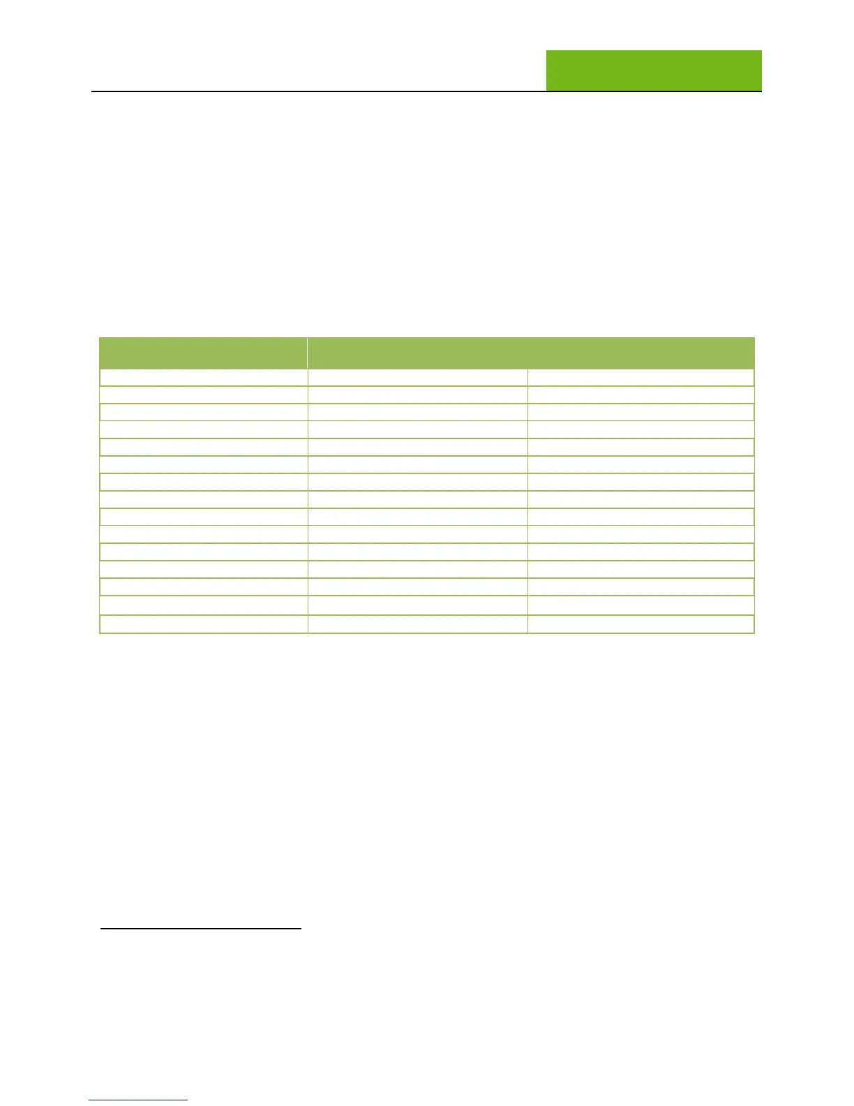
The following table provides a high-level comparison of Maxwell vs. our previous-generation GK104
GPU:
GeForce GTX 980 (Maxwell)
The GeForce GTX 980 has double the SMs compared to the GK104 GPU used in the GeForce GTX 680
released two years ago. Because of the changes implemented in GTX 980’s new Maxwell SM, we were
able to integrate 2x more SMs without doubling the die size. With each SM also containing its own
dedicated PolyMorph Engine, GeForce GTX 980 also has twice the number of geometry units as its direct
predecessor. We’ll be discussing more details on the new SM design in the next section of the
whitepaper.
Based on efficiency and workload analysis, and math vs. texture processing requirements of modern
games, NVIDIA engineers determined that eight texture units per SMM is the best architectural balance
for Maxwell; therefore, the total number of texture units is the same as Kepler, 128. However, thanks to
GeForce GTX 980’s higher clocks, texture fill rate improves by 12% from one generation to the next. To
improve performance in high AA/high resolution gaming scenarios, we doubled the number of ROPs
The GFLOPS and texel fill rates in this chart are based on GPU Base Clock