NXP Semiconductors
UM12018
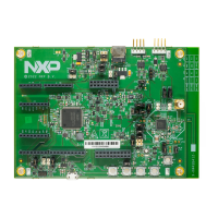
FRDM-MCXN947 Board User Manual
Pin
number
Device
pin / GPIO
Function / Signal name Resistor setting Potential conflict
17 P1_0 TSI0_CH0 - • mikroBUS header J5 pin 6 (P1_
0/FC3_I2C_SDA)
• MCU-Link USB bridge (P1_0/
FC1_SPI_SDO_MCULINK)
P4_0 FC2_I2C_SDA-ARD_D18 SJ14 Pin 1-2 selection
(default setting)
-18
P1_16 I3C1_SDA SJ14 Pin 2-3 selection • Camera connector J9 pin 4
(P1_16/EZH_LCD_D12)
• mikroBUS header J5 pin 3 (P1_
16/ME_FC5_RXD)
19 - - - -
P4_1 FC2_I2C_SCL-ARD_D19 SJ15 Pin 1-2 selection
(default setting)
-20
P1_17 I3C1_SCL SJ15 Pin 2-3 selection • Camera connector J9 pin 3
(P1_17/EZH_LCD_D13)
• mikroBUS header J5 pin 4 (P1_
17/ME_FC5_TXD)
Table 18. Arduino compatible header J2 pinout...continued
Pin
number
Device pin /
GPIO
Function / Signal name Resistor setting Potential conflict
1 P2_0 TRIG_IN5-MC_ENC_B - Camera connector J9 pin 25 (P2_
0/EZH_LCD_WR through the
zero-ohm resistor R167)
2 ANA_6 ADC0_A3 - -
3 P1_22 TRIG_IN3-MC_ENC_A - Camera connector J9 pin 24 (P1_
22/EZH_LCD_DC)
4 - P3V3 - -
5 P2_3 PWM1_B2 - SD card connector (J12) pin 7
(SDHC0_D0)
6 RESET_b RESET_B - -
7 P2_2 PWM1_A2 - SD card connector (J12) pin 8
(SDHC0_D1)
8 - P3V3 - -
9 P2_5 PWM1_B1 - SD card connector (J12) pin 3
(SDHC0_CMD)
10 P5V0 - - -
11 P2_4 PWM1_A1 - SD card connector (J12) pin 5
(SDHC0_CLK)
12 GND - - -
13 P2_7 PWM1_B0 - SD card connector (J12) pin 1
(SDHC0_D2)
14 GND - - -
Table 19. Arduino compatible header J3 pinout
UM12018 All information provided in this document is subject to legal disclaimers. © 2024 NXP B.V. All rights reserved.
User manual Rev. 1 — 20 January 2024
23 / 41
 Loading...