DC Power Distribution
+12VDC Output
For an illustration of the PS1 +12VDC output, refer to the following diagram:
PS1
Power/Motor Relay PCB
TP16
+12V
TP14
Voltage
Dropping
Resistor
Array
F5
F4
F2
F3
P10
2
P11
4
P12
1
4
P8
7
J2
8
X-Ray
Tube
Cooling
Fan
IGBT Fan
Backplane
Fluoro Functions PCB
(No Connection)
P5
9
COOLER_SPLY
A3J1
26
CCD
Camera
Cooler
Power
3
No Connect
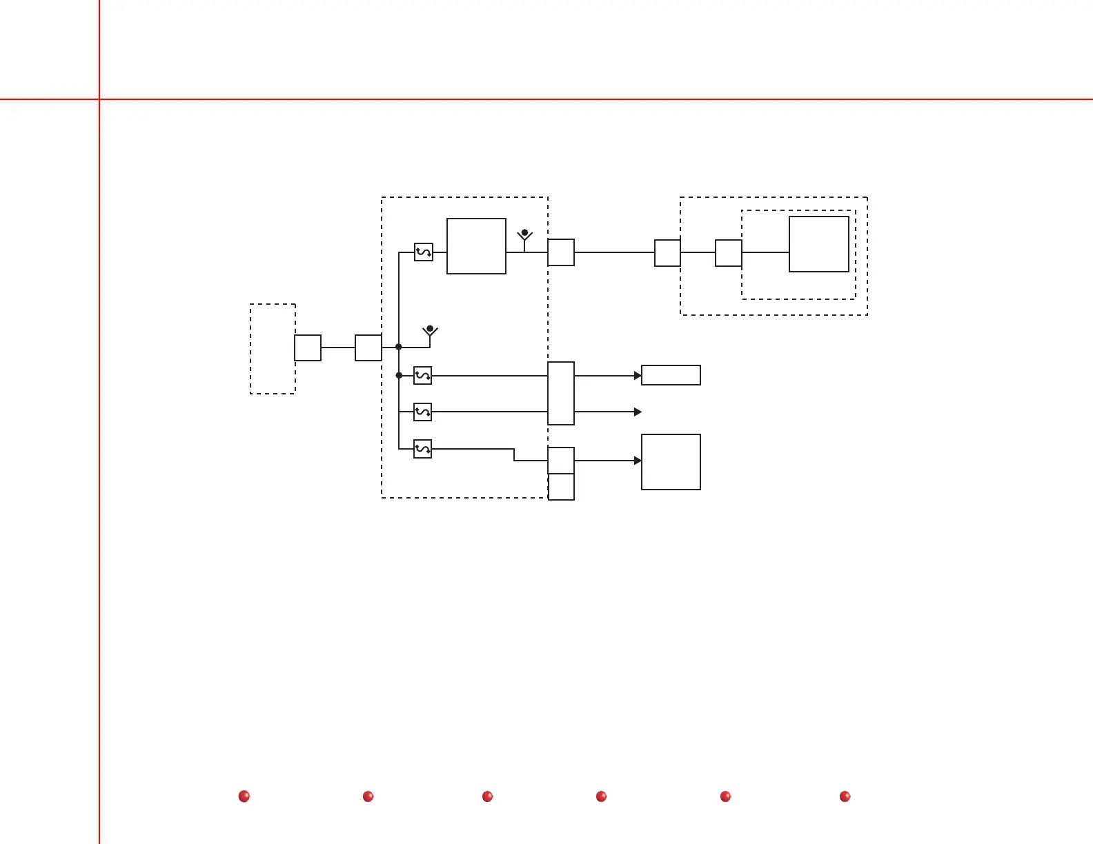
PS1 +12VDC Output
PS1 provides one line of +12VDC to Connector P8 of the Power/Motor Relay PCB, where it divides into separate circuits
protected by Fuse F2, F3, F4, and F5. F2 connects to P12-4, and is not used. F3 connects to P12-1, which in turn goes to the
IGBT PCB fan. F4 leaves the board via Connector P11, providing power to the X-ray tube cooling fan. F5 is processed by a
voltage dropping resistor array, and exits the board via Connector P10 as COOLER_SPLY, going to the CCD Camera cooling
control circuitry.
6
Service
Periodic Maintenance
Contents
Schematics
Illustrated Parts
Installation