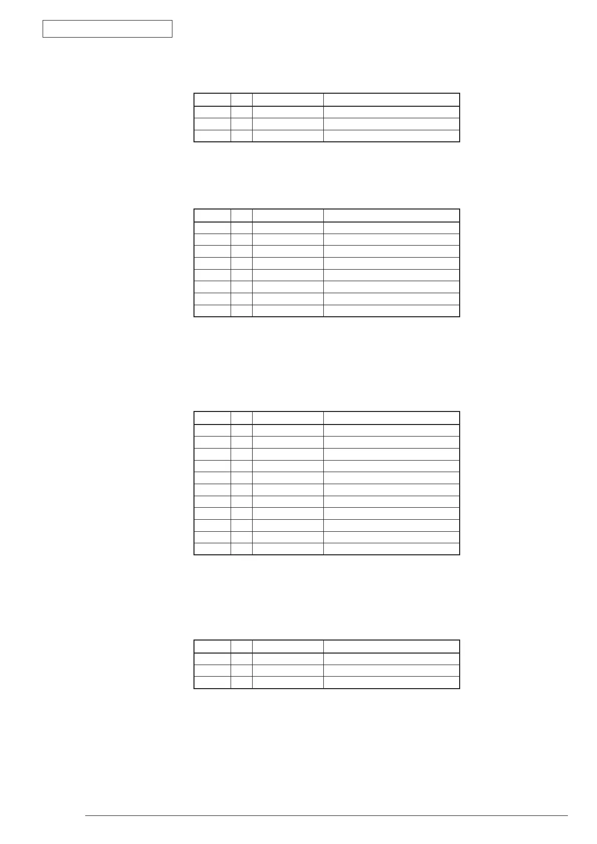
7. Connection Diagram
Oki Data CONFIDENTIAL
44983601TH Rev.1
7-10 /
• PAPConnectorPinAllocation
(ConnectiontothePhotointerrupter)
• 2NDConnectorPinAllocation
(ConnectiontotheOptiontrayI/F)
PinNo. I/O Signal Function
1 O +5V LogicCircuitPowerSupply
2 I PAPER-N PaperendSensorsignalinput
3 C GND Logic Ground
PinNo. I/O Signal Function
1 O FANPOW FANDrivePower
2 C FANGND AnalogGround
3 I FANALM FANAlarmDetection
PinNo. I/O Signal Function
1 C 0VP AnalogGround
2 O +24V Motor/ClutchDrivePower
3 C 0VL Logic Ground
4 O +5V LogicCircuitPowerSupply
5 I OPTRXD OPTdatainput
6 O OPTTXD OPTdataoutput
7 I OPINT-N OPTstatuschange
8 O OPTFDEN-P OPTtransferpermission
PinNo. I/O Signal Function
1 O HARD_GUARD Hard Guard
2 O ACON1-P HeaterON
3 I +5V LogicCircuitPowerSupply
4 I +5V LogicCircuitPowerSupply
5 C 0VL Logic Ground
6 C 0VL Logic Ground
7 O ACZEROX ACZeroCross
8 C 0VP AnalogGround
9 C 0VP AnalogGround
10 I +24V Motor/FAN/ClutchDrivePower
11 I +24V Motor/FAN/ClutchDrivePower
• POWERConnectorPinAllocation
(Connectiontothelow-voltagepowersupply)
• DFAN1ConnectorPinAllocation
(ConnectiontotheMotor-Fan(Duct))