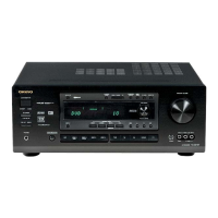
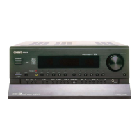
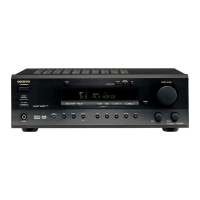
TX-DS797
MAIN MICROPROCESSOR
Terminal Descriptions
TX-DS797
No. Function I/O Act. Description No. Function I/O Act. Description
8 BYTE I Input pin to change the width of external data bus. Connect to Vss. 52 ADR152 O H Signal output pin to control address 15 of flash memory for second DSP.
9 CNVSS I Input pin to change the processor mode. Connect to Vss. 53 ADR162 O H Signal output pin to control address 16 of flash memory for second DSP.
12 ~RESET I Reset pin of microprocessor 54 ADR172 O H Signal output pin to control address 17 of flash memory for second DSP.
13 XOUT O Output pin of main clock oscillator 55 DFSDAC O H DAC sampling control output pin.
14 VSS I Ground pin 56 ~DARST O L Reset output pin for six channels DAC.
15 XIN I Input pin of main clock oscillator 57 ~CODECPD O L Reset output pin for CODEC IC.
16 VCC I Power supply pin. Apply 5V. 58 DFSCO O H Sampling frequency control output pin for CODEC IC.
18 PRTCTV I H Abnormal voltage/current detection input pin from protection circuit 62 VCC I Power supply pin. Apply 5V.
19 RDSSCK I CLK Modulator clock signal input pin from RDS decoder IC. 64 VSS I Power supply pin. Connect to ground,
20 ~POFF I L Input pin from detection circuit of power failure 68 TRG12A O H Output pin A to control the 12V trigger circuit.
21 ~PRTCTTHM I L Input pin from thermal detector circuit. 69 TRG12B O H Output pin B to control the 12V trigger circuit.
22 SEC1H O H Output terminal to change voltage of main amplifier. 70 TRG12Z O H Output pin to control the 12V trigger circuit of zone 2.
23 INT0 I H Input terminal from interrupter output of DIR IC. 71 SPRLZ2 O H Output pin to control the speaker relay of zone 2.
24 INT1 I H Output terminal to interrupter input of DIR IC. 72 SLRLF O H Output pin to control the speaker relay.
25 (DSPWRITE) I L Input port for check when DSP flash write. 73 POWER O H Output pin to control the relay of power source.
26 DIGSO O H Serial data output pin to DSP,DIR,DAC, nd Digital input ICs. 74 PLLCE O H Latch data output pin to PLL IC.
27 DIGSI I H Serial data input pin from DSP, and DIR ICs. 75 TUMUT O H Muting control output pin for tuner block.
28 DIGSCK O CLK Serial clock output pin to DSP,DIR,DAC,Digital input ICs. 76 ~SD I L Signal detection input pin from tuner section.
29 ~INTRQ1 I L INTRQ input pin from DSP IC 2(CS49329) 77 ~STEREO I L Stereo broadcast detection input pin.
30 ~INTRQ2 I L INTRQ input pin from DSP IC 1(CS49300) 78 RDSDATA I H Data input pin from RDS demodulator IC.
32 ~SUBRESET O L Reset signal output pin to sub-microprocessor. 79 RDSSIG I H Check signal input pin of RDS demodulator IC.
33 ~SUBPOFF O L Output pin to connect to pin POFF of sub-microprocessor. 81 AMUT O H Muting control output pin for audio circuit.
34 ~SUBREQ I L Communication request input pin from sub-microprocessor. 82 Z2LMUT O H Muting control output pin for line of zone 2.
35 MAINSO O H Serial data output pin to sub-microprocessor. 83 Z2MUT O H Muting control output pin for zone 2.
36 MAINSI I H Serial data input pin from sub-microprocessor. 84 VPCLK O H Serial clock output pin to electrical volume and PLL IC,
37 MAINSCK O CLK Serial clock output pin for communication of main and sub-microprocessors. 85 VPDATA O H Serial data output pin to electrical volume and PLL IC,
38 ~MAINREQ O L Communication request output pin of main microprocessor. 86 VSTB O H Strobe output pin to electrical volume IC.
39 ~DIRCS O L Chip select output pin of DIR IC, 87 TCS2 O L Chip select output pin to tone control IC of surround and center channels.
40 ~DIRRST O L Reset signal output pin to DIR IC, 88 TCS1 O L Chip select output pin to tone control IC of front channel..
41 Writing port of flash memory IC. 89 TDATA O H Serial data output pin to tone control IC.
42 ~DSPRST1 O L Reset signal output pin to DSP IC 2. 90 TCLK O CLK Serial clock output pin to tone control IC.
43 ~DSPCS1 O L Chip select output pin to DSP IC 1. 91 FSTB O H Strobe output pin to function switch ICs.
44
FMEM/SRAM1
O H Memory select output pin to RAM. 92 FDATA O H Serial data output pin to function switch ICs.
45
ADR151
OHSi
Serial clock output pin to function switch ICs.
46 Port to write the flash memory IC. 94 HPMUT O H Muting control output pin for headphone circuit.
47 ADR161 O H Signal output pin to control address 16 of flash memory for first DSP. 96 VSS I Power supply pin for A/D converter. Connect to ground.
48 ADR171 O H Signal output pin to control address 17 of flash memory for first DSP. 97 VOLH I H Measurement input pin of main amplifier output.
49 ~DSPRST2 O
L
Reset output pin to DSP IC 2. 98 VREF I Reference voltage input pin for A/D converter.
50 ~DSPCS2 O L Chip select output pin to DSP IC 2. 99 VCC I Power supply pin for A/D converter. Apply 5V.
51
FMEM/SRAM2
O H 2nd DSP memory select output pin.L=FLASH,H=SRAM
 Loading...