RMX Series Technical Service Manual 7
the transistor pair to keep crossover distortion minimal. In parallel
with the trimpot is a 50-ohm thermistor with a negative temperature
coefficient; as the circuitry warms, its resistance decreases. This
reduces V
BE
on both Q105 and Q106, decreasing the bias current to
reduce the threat of thermal runaway. The base of each driver transistor
is tied to ground through a diode and a 2.2K trimpot in series; these set
the current limiting threshold for their respective signal polarities.
The collector of each driver transistor directly drives the bases of its
output transistors, which are the main power-handling signal
devices. If you’re not familiar with the grounded-collector scheme,
the arrangement of the output transistors might look somewhat
strange: the positive voltage swings are handled by PNP transistors,
while the negative swings are handled by NPN devices. The
collectors all connect to ground, which allows them to be mounted
directly to the heat sink—metal-to-metal, without insulators in
between—for the best possible transfer of heat away from the
transistors. The emitters of the PNP and NPN transistors are
coupled through resistors to the positive and negative supply rails,
respectively, forming banks of common-emitter circuits driving the
supply rails. Consequently, the devices drive the rails with the audio
signal, which rides atop the DC. The output to the speaker load is
taken from the point between the positive and negative reservoir
capacitors; this is also where the negative feedback is taken from.
The nature of this arrangement, with audio signal riding on the
supply rails, is why the power supply has no ground reference.
Another unusual characteristic of the grounded-collector output
section is that the signal at the output to the speaker is actually
opposite in polarity to the signal at the op amp output. This is why
the negative feedback resistor, R122, connects to the op amp’s non-
inverting input instead of the inverting input.
The output point of the circuit couples to the output connector
through an RLC network (R160, R161, R162, L100, and C124) that
serves as a high-frequency snubber and also helps keep the amp
circuitry stable when driving capacitive loads.
R111
100
^R_0805
R109
100
^R_0805
10.0K
^R_0805
R103
3
+
8
7
5
1
4
-
2
U10:1
LM13600M
R108
7.50K
^R_0805
+14V
A1
R104
150K
^R_1206
-14V
R110
270
^R_0805
C105
100-25V
R107
^R_0805
39K
Q100
3906
R115
820
^R_1206
To input op amp U101:1
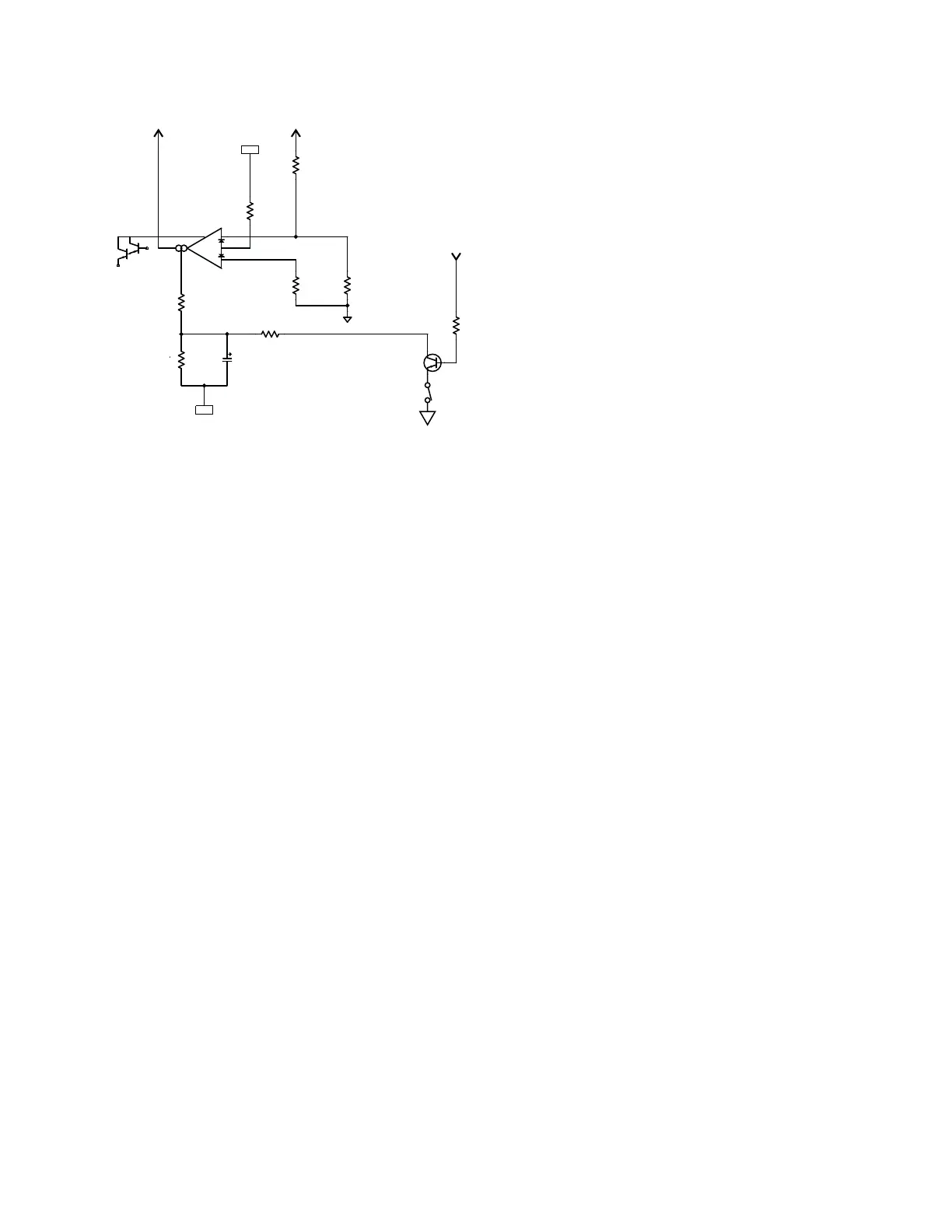
11
CLIP LIMIT
SWITCH
(Open to defeat
clip limiter)
From clip
detection
Clip detection
The output of the op amp also drives a group of four diodes (D102,
D103, D105, and D106) arranged as a full-wave rectifier. Normally,
the op amp’s output signal level is about 1 volt or less, which is all it
takes to drive the driver transistors.
But because this point is within the overall feedback loop, when
clipping occurs, the op amp puts out a much higher signal voltage to
try to make the output signal track the input. The four diodes rectify
the voltage to drive the clip indicator LED, LD100. The current
exiting the full-wave rectifier passes to ground through R127 and
also drives the base of transistor Q100 through R115. If the clip
limiter is switched on, Q100’s emitter is grounded, and when the
voltage across R127 goes sufficiently negative to forward-bias
Q100, which sends current through R111 and R103 into the amplifier
bias input of the operational transconductance amplifier (OTA),
U10:1. The OTA is in the negative feedback loop of U101:1, and
increasing its transconductance essentially reduces the impedance
of the feedback loop, which reduces the gain of the op amp stage.
This reduces the signal level until the amount of clipping is minimal.
When the clipping stops, Q100 is no longer forward-biased, and the
gain returns to normal.
DC protection
The RMX 2450 has a crowbar circuit, based on a triac and two
silicon controlled rectifiers, on the output to protect against DC
faults. If an amp channel puts out a DC voltage, which could be the
result of a component or circuit failure, it will first trigger either
D119 or D120, depending on the polarity of the voltage. The
triggered SCR will in turn trigger triac Q113, shorting the output to
ground through fuse F100. The fuse will blow, safeguarding the
speaker load from the DC fault.
The output sections of the RMX 850 and RMX 1450 are AC coupled.
Class H
The RMX 2450 utilizes a two-step Class H output section. It is
essentially a Class AB+B circuit but with two sets of bipolar supply
rails. On both the positive and the negative sets of rails, a compara-
tor circuit, called a “step driver,” compares the audio signal to the
lower rail voltage. When necessary to fully reproduce the signal’s
voltage swing—just before the signal voltage reaches the lower rail
voltage—the step driver turns on a TMOS power FET to pull the
output transistors’ supply rail up from the lower voltage to the
higher one, and then back down again when the signal allows. By
keeping the transistors’ supply rails low whenever possible, the
devices dissipate less unused power and generate less waste heat,
making the amplifier more efficient than a straight class AB
amplifier with the same power points.
The comparators are 311-type ICs: U170 on the positive step and
U171 on the negative. Each one drives a high-gain complementary
transistor pair (2N3904 + 2N3906), which drive the gate of their
respective MOSFET.
Figure 1.10