High−level Instructions
3 − 145
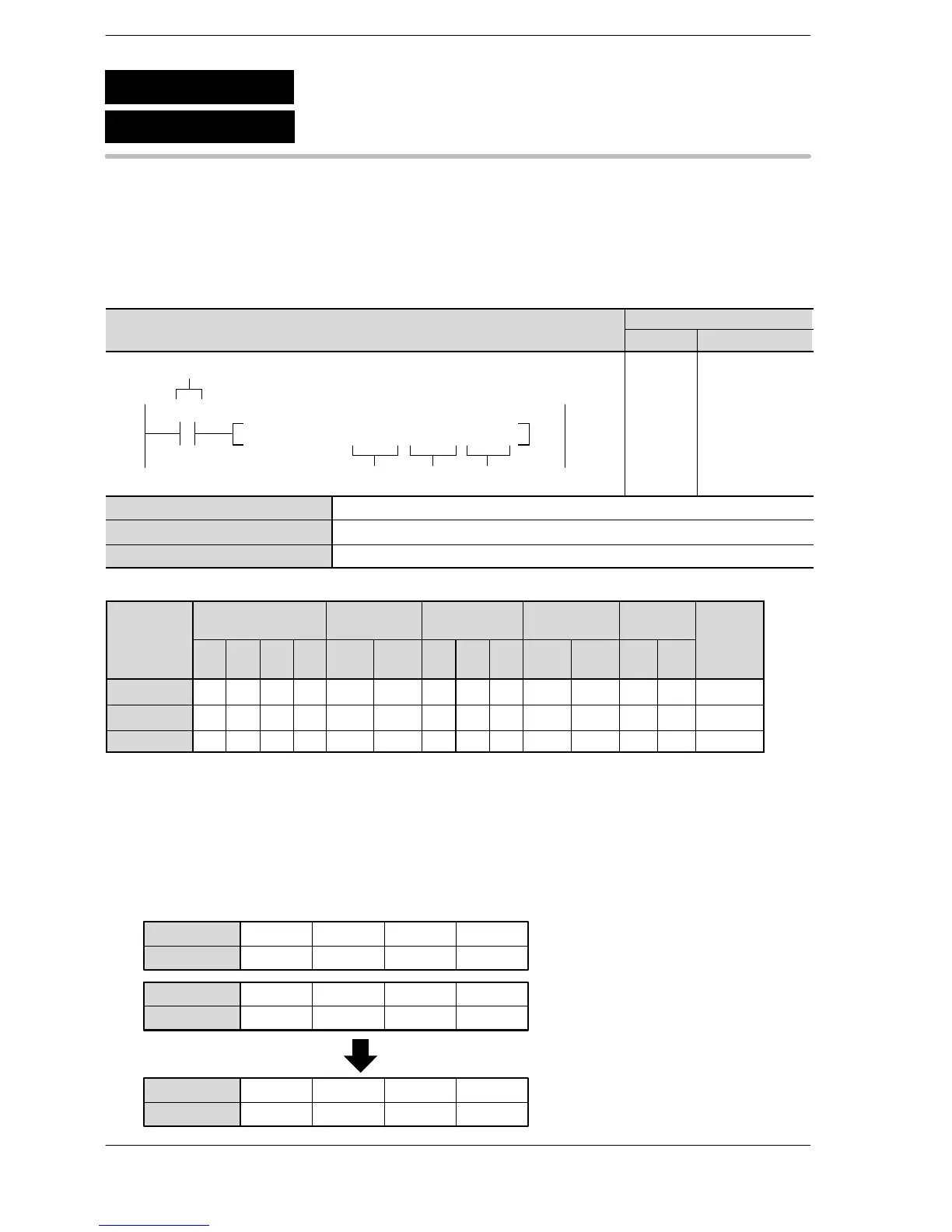
Outline Performs bit-wise OR operation on two 16-bit data items.
For the FP0R/FPΣ/FP−X/FP0/FP−e, the P type high−level instruction
“P66 (PWOR)” is not available.
Program example
Boolean
Ladder Diagram
Address Instruction
10
F66 WOR , DT10 , DT20 , DT30
S1
D
Trigger
S2
R0
10
11
ST R 0
F66 (WOR)
DT 10
DT 20
DT 30
S1 16-bit equivalent constant or 16-bit area
S2 16-bit equivalent constant or 16-bit area
D 16-bit area for storing OR operation result
Operands
modifier
S1 A A A A A A A A A A A A A A
S2 A A A A A A A A A A A A A A
D N/A A A A A A A A A A A N/A N/A A
(*1) This cannot be used with the FP0 and FP−e.
(*2) This cannot be used with the FP0, FP−e, FP0R, FPΣ, FP−X.
(*3) With the FP0R, FPΣ,FP−X, FP2, FP2SH, and FP10SH, this is I0 to IC.
(*4) With the FP0R, FPΣ,FP−X, FP2, FP2SH, and FP10SH, this is ID.
Explanation of example
Performs OR operation on each bit in data registers DT10 and DT20 when trigger R0 turns on.
The OR operation result is stored in data register DT30.
[S1]
[S2]
[D]
····
Bit position
·····
DT10
15
010
12
0
11
110
8
1
7
101
4
1
3
100
0
1
R0: on
····Bit position ·····
DT20
15
000
12
0
11
000
8
0
7
111
4
1
3
111
0
1
····Bit position ·····
DT30
15
010
12
0
11
110
8
1
7
111
4
1
3
111
0
1
F66
P66
(PWOR)
(WOR)
16-bit data OR
A: Available
N/A: Not Available





 To Next Page