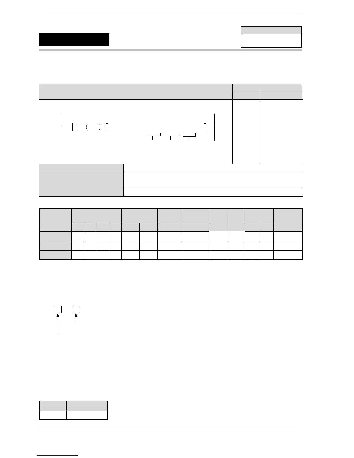
Boolean
Ladder Diagram
Address Instruction
DF
F166 HS1S , H100, K10000, Y2
R0
D
Sn
10
11
12
ST R 0
DF
F166 (HC1S)
H 100
K 10000
Y2
n The channel number of the pulse output that corresponds to the match output.
S
The pulse output target value data or the starting address of the area that
contains the data.
D The output coil that is turned on when the values match. (Yn)
Operands
O
K H
modifier
n N/A N/A N/A N/A N/A N/A N/A N/A N/A N/A A A N/A
S A A A A A A A A N/A N/A A A A
D N/A N/A N/A N/A N/A N/A N/A N/A N/A N/A N/A N/A N/A
(*1) I0 to ID
Description
The number specified in “S” is set as the target value of the pulse output channel, and when the elapsed value
matches the target value, the specified output “Yn” turns on (by interrupt processing).
Specify the channel number of the pulse output in “n”.
H0 1 0 0
<Specification of the channel of high−speed counter/pulse output>
Allowable range for specifying the pulse output: 0 to 3
<Specification of high−speed counter/pulse output>
1: Specification of pulse output
The target value setting and target value match output control are cleared when the elapsed value matches
the target value. The control flag also turns off.
Specify a 32−bit data value for the target value “S” within the following range:
FP0R K−2,147,483,648 to K2,147,483,647
The “S” value is stored in the target value area when the instruction is executed.
Possible specification range for “Yn”: Devices specified for the match ON/OFF output
Type
Device area
FP0R Y0 to Y1F
FP0R
Target value match on
(Pulse output control)
F166
(HC1S)
Availability
FP0R
A: Available
N/A: Not Available
However, for the device that is not implemented, only the memory turns ON/OFF.





 To Next Page