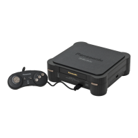
FZ-10
IC400
Continued {IC120)
Backup Controller
(PIN:
DABA6162FT2E}
Pin
No.
1/0
Pin Name
Comment
Pin
No.
1/0
Pin Name Comment
286 I CDCLK
CD
interface
clock
1 N/C
(Not Connected)
287 I
CREF Clock reference
input
2 Out VREF
Voltage Reference Output
288 0
LPSO'
Tracking signal
of
left
serial
clock
3
N/C
(Not Connected)
289 0
RPSO'
Tracking signal
of
right
serial
clock
4
AVDD
Analog Power suoolv
290 I
PON
Power-on signal.
PON
is high and
5 AVSS
Analoq qround
stabe whenerver the system is on
6 Input
TST
Test pin
291
0
PCSO'
Output
to
indicate the beginning
of
7 Input
LRCK
UR Clock input
a scan line
8 Input
BICK Serial data clock
292
GND Ground
293
VDD
Power supply
IC600
294
AVDD
Analog power supply
CD-ROM Interface Gate Array
: (P/N DA623854PVJ)
295 AGND
Analog ground
Pin
No.
1/0
Pin
Name Comment
296 I
VREF1
Voltage reference input.
Nomally
1 Out
COEN-
CD
drive enable
1.5V
2
GND
Ground
297
0
CGAIN
Chroma full-scale current control
31/0
CDD7
CD
drive data bus 7
298
0
YGAIN Luminance full-scale current
41/0
CDD6
CD
drive data bus 6
control
51/0
CDD5
CD
drive data bus 5
299 I CCOMP
Chroma compensation
6
l/0
CDD4
CD
drive data bus 4
300 I
YCOMP
Luma DAC compensation
71/0
COD3
CD
drive data bus 3
301
I
VREFO
Voltage reference input.
Nomally
1.75V
302 AGND
Analog ground
303
0
COUT
Chrominance video signal
304
0
BLUE
Blue
output
when ANVIL video
DAG
is in the
RGB
mode
81/0
CD02
CD
drive data bus 2
91/0
CDD1
CD
drive data bus 1
10
l/0
CDDO
CD
drive data bus 0
11
Out
CDRST-
CD
drive reset
12
GND
Ground
13
Input
CLK33M 33MHz clock
14
Input
ROMSEL
ROM
selection
15
Input
ROMEN
ROM
enable
16 Out ROMA20
ROM
address 20
17
Out
ROMEO-
ROM
output enable 0
18 Out ROME1-
ROM
output enable 1
19
Out ROMCS-
ROM
chip selection
20
Input CPURES-
CPU
reset
IC200
21
1/0
EDO
Internal expansion bus 0
Audio DAC (P/N: DA4310VME2XQ)
22
1/0
ED1
Internal expansion bus 1
Pin
No.
1/0
Pin Name Comment
23 GND
Ground
1 Input
TST1
Test pin
24
l/0
ED2 Internal expansion bus 2
2
DVDD Digital
5V
25
l/0
ED3
Internal expansion bus 3
3
DVSS
Digital ground
26
1/0
ED4 Internal expansion bus 4
4 Input
PD-
Power down signal
input
27
1/0
EDS
Internal expansion bus 5
5 Input
RST-
Reset pin
28
l/0
ED6
Internal expansion bus 6
6 Input MCLK Master
clock
pin
29
1/0
ED7 Internal expansion bus 7
7 Input
CKS Clock selection (H: 256fs, L: 384fs)
30
Input ESTA-
Internal strobe
8 Input BICK Serial
bit
clock
31
Input EWRT-
Internal write
9 Input
SDATA
Serial
data
input
32
Input
ERST- Internal reset
10 Input LACK L/R chanel
clock
33
VDD
Power supply
11
N/C
Not
connected
34
Input
ECMD-
Internal command
12 N/C
Not
connected
35
Input
ESEL- Internal selection
13
N/C
Not connected
36 Tri-Out EADY- Internal ready
14
N/C
Not
connected
37
Tri-Out EINT- Internal interrupt
15 Output AOUTR
Reh Analog
output
38
Input
!DIN
ID
input from previous device
16 Output AOUTL Leh Analog
output
39 Out AND
AND
output (pins
43
and 44\
17 Output VCOM Common voltage, AVDD/2
40
Out
XACLK Audio reference clock
18
AVDD Analog power supply
41
Out
NANO NANO
output (pins
43
and
44)
19 AVSS Analog ground
42
GND
Ground
20
N/C Not connected
43
Input
A
General input A
21
N/C
Not connected
44
Input
B General input B
22 Input VREFH Reference voltage (High level)
45
Out XRST- External bus reset
VREFH and VREFL determin full
46
Out IDOUT
ID
output
scale
of
D/A
output
47
Input
XDIN
ID
input
23
Input VREFL
Reference voltage (Low level)
48
Out XWRT- External bus write
24 Output
DZF
Zero detect
49
Out XSEL-
External bus selection
2-10
 Loading...