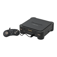
FZ-10
Continued (IC120) Continued (IC120)
Pin
No.
1/0 Pin Name Comment
Pin
No.
1/0 Pin Name Comment
193 1/0 ADBlO2 General-purpose 1/0 bus 2 239 I
A9
ADDRESS 9
194 1/0 ADBIO3
General-purpose 1/0 bus 3
240 I A10
ADDRESS
10
195 0 AUDBCK
Audio
bit
clock
241
I
A11
ADDRESS
11
196 1/0 AUDWS
Audio
channel selection 242 I A12 ADDRESS 12
197
VDD Power
supply
243 I A13 ADDRESS13
198 1/0
PD0
Bi-directional
data
bus
for
the
slow
244 I A14 ADDRESS14
bus 0
245 GND Ground
199 1/0
PD1
Bi-directional
data
bus
for
the
slow
246 I A15 ADDRESS 15
bus 1
247 I A16 ADDRESS 16
200 1/0
PD2
Bi-directional
data
bus
for
the
slow
248 I A17 ADDRESS 17
bus 2
249 I A18
ADDRESS 18
201
1/0
PD3
Bi-directional
data
bus
for
the
slow
250 I A19
ADDRESS 19
bus
3
251
I A20 ADDRESS
20
202
GND
Ground
252 I
A21
ADDRESS
21
203 1/0
PD4
Bi-directional
data
bus
for
the
slow
bus 4
204 1/0
PD5
Bi-directional
data
bus
for
the
slow
bus 5
205 1/0
PD6
Bi-directional
data
bus
for
the
slow
bus 6
253 I A22 ADDRESS
22
254 I A23 ADDRESS
23
255 I A24 ADDRESS
24
256
VDD Power
supply
257 I A25 ADDRESS
25
206 1/0
PD7
Bi-directional
data
bus
for
the
slow
258 I A26 ADDRESS 26
bus 7
259 I TRANS*
Indicator
that
the
CPU
is in user
207 VDD
Power
supply
208 1/0
EDD
Bi-directional address annd
data
mode
260 0 CPURE&
CPU
reset signal
bus
for
the
expansion bus 0
261
0 FIRQ*
CPU
interrupt
209 1/0
ED1
Bi-directional address annd
data
262 GND Ground
bus
for
the
expansion bus 1
263 0 ABORT
CPU
abort signal.
This
signal
210 1/0
ED2
Bi-directional address annd
data
become H when a memory access
bus
for
the expansion bus 2
is
not
possible
211
1/0
ED3
Bi-directional address annd
data
264 I
SEQ
Indicator
of
a sequential memory
bus
for
the expansion bus 3
access
212 GND Ground
265
0
MCLK Master
CPU
clock
213
1/0
ED4 Bi-directional address annd
data
266 GND Ground
bus
for
the
expansion bus 4
267 I XIN Crystal
input
for
the system
clock
214 1/0
ED5
Bi-directional address annd
data
268 0 XOUT
Crystal
output
for
the system
clock
bus
for
the
expansion bus 5
269 GND Ground
215 1/0
ED6
Bi-directional address annd
data
270 I MREQ*
Indicator
that
the
CPU
requires
bus
for
the expansion bus 6
memory access
216 1/0
ED7
Bi-directional address annd
data
271
I READ*
Indicator
of
the
CPU
Read/Write
bus
for
the expansion bus 7
status
217
1/0
CREADY* Device
control
hand shake signal
272 I BYTE* The
CPU
tells
ANVIL which
data
218 1/0
RTC
type is required, 8
bit
(L)
or
32
bit
(H)
219 1/0
HS*
Horizontal
sync
273 VDD
Power supply
220 1/0
V&
Vertical
sync
274 0 DBE Data bus enable
221
VDD Power
supply
222 I AUDIN
Input
data
from AID converter
223 I PDINT'
Slow bus level-sensitive
interrupt
224 I
EXTREQR
Audio DMA read request signal
225 I
EXTREQW
Audio DMA
write
request signal
226 I
UNCREQR
Video DMA read request signal
227 I
UNCREQW
Video DMA
write
request signal
228 GND Ground
229 I
AO
ADDRESS 0
230 I
A1
ADDRESS 1
231
I A2 ADDRESS 2
275 I LOCK
Indicator
that
the
CPU
is
performing a locked memory
access and
that
ANVIL
must
wait
276 0 EWRT' Write signal
for
the expansion bus
277 0
ESTR*
Strobe signal
for
the expansion bus
278 GND Ground
279 I EINT' Interrupt signal from expansion
device
280 0 ERST'
Power-on and software-controlled
reset signal
to
the expansion bus
281
0 ESEL* Selection signal
for
the expansion
bus
232 I A3 ADDRESS 3
233 I
A4
ADDRESS 4
282 0
ECMD* Command signal
for
the expansion
port
234 I
A5
ADDRESS 5
283 VDD Power
supply
235 VDD
Power
supply
284 I
ERDY*
Ready signal from expansion
236 I
A6
ADDRESS 6
device
237 I
A7 ADDRESS 7
285
I CDDATA
CD
interface
data
238 I
AB
ADDRESS 8
2-9

 Loading...