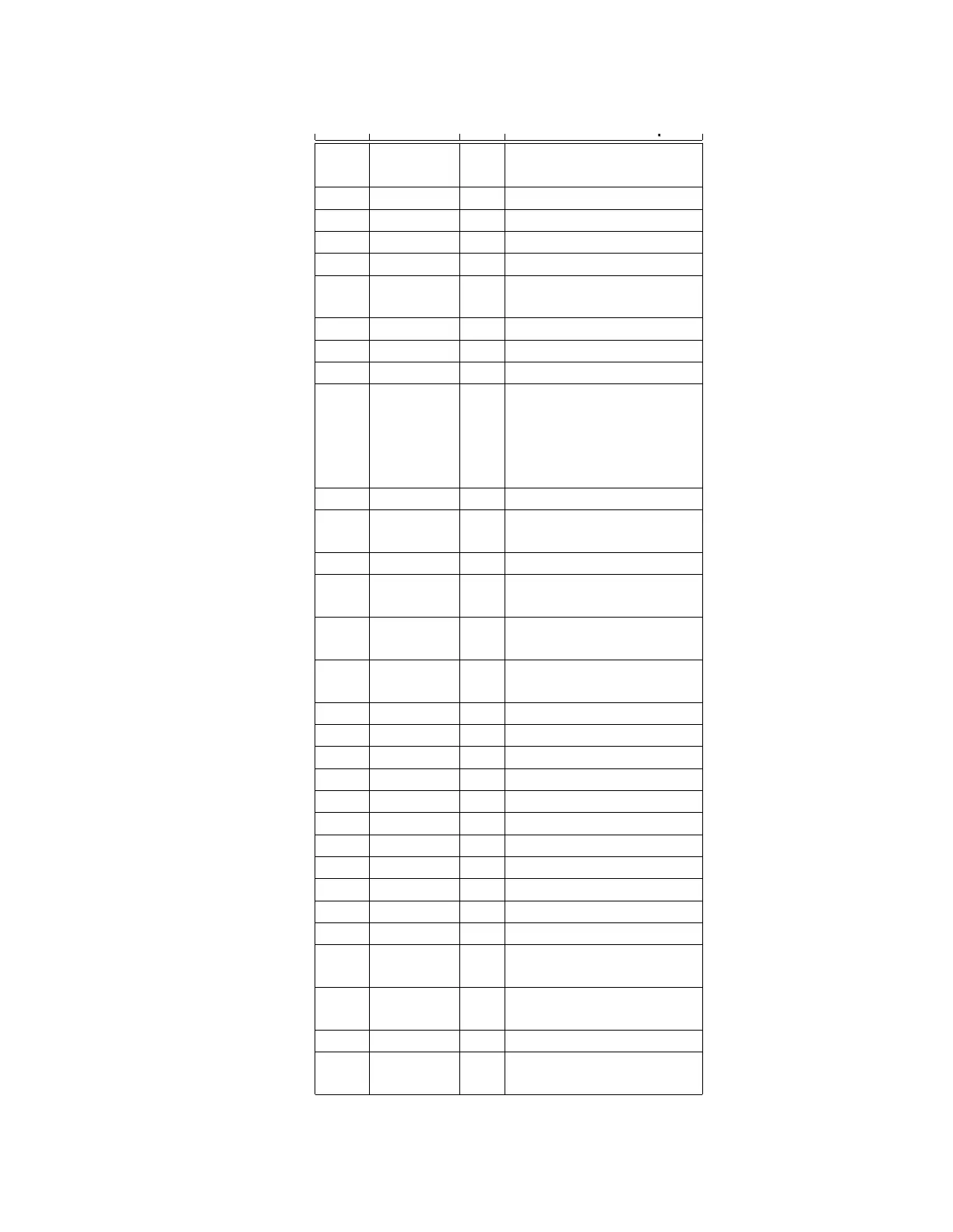
Pin
No.
Mark I/O Function
46 DRF I DSL bias terminal
47 DSLF I/O DSL loop filter terminal
48 PLLF I/O PLL loop filter terminal
49 VCOF I/O VCO loop filter terminal
50 AVDD2 I Power supply input (for
analog circuit)
51 AVSS2 I Gnd (for analog circuit)
52 EFM - N.C.
53 PCK - N.C.
54 VCOF2 I/O VCO Loop filter for
33.8688MHz conversion
terminal for 16.9344MHz
crystal mode, must use
other circuit
55 SUBC - N.C.
56 SBCK I Clock input for sub-code
serial data
57 VSS I Gnd
58 X1 I Crystal oscillating circuit
input (f = 16.9344MHz)
59 X2 O Crystal oscillating circuit
output (f = 16.9344MHz)
60 VDD I Power supply input (for
oscillating circuit)
61 BYTCK - N.C.
62 /CLDCK - N.C.
63 FCLK - N.C.
64 IPFLAG - N.C.
65 FLAG - N.C.
66 CLVS - N.C.
67 CRC - N.C.
68 DEMPH - N.C.
69 RESY - N.C.
70 IOSEL I Mode Switching Terminal
71 /TEST I Test input
72 AVDD1 I Power supply input (for
analog circuit)
73 OUTL O Left channel audio signal
output
74 AVSS1 I Gnd
75 OUTR O Right channel audio
signal output
40