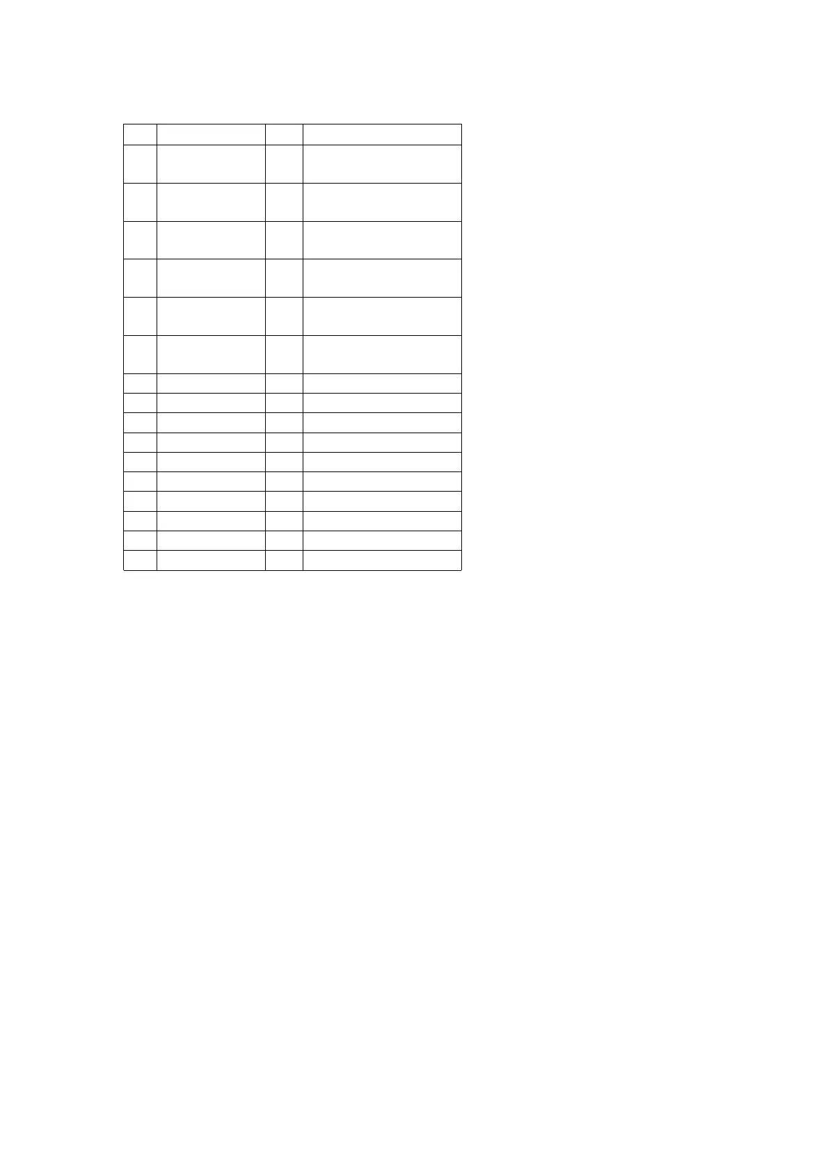
No. Mark I/O Function
47 CHG_CCW O Changer motor CCW
output
48 CHG_CW O Changer motor CW
output
49 VJOG_B I Main volume jog input
B
50 VJOG_A I Main volume jog input
A
51-
55
N.C. O No connection
56-
90
SEG34-SEG0 O Segment drive output
91 VCC - Power supply (+5V)
92 VREF - Reference for A-D
93 AVSS - Analog ground (0V)
94 COM3 - LCD common 3 output
95 COM2 - LCD common 2 output
96 COM1 - LCD common 1 output
97 COM0 - LCD common 0 output
98 VL3 - LCD Bias
99 VL2 - LCD Bias
100 N.C. - OPEN
14. Block Diagram
15. Schematic Diagram
(All schematic diagrams may be modified at any time with the development of the new
technology)
Note:
S601
: Power switch
S602
: Clock/Timer /Demo switch
S603
: Rec/ Play/ Demo switch
S604
: Disc 1 switch
S605
: Disc 2 switch
S606
41