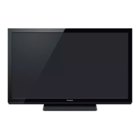
Do you have a question about the Panasonic TC-P54V10 and is the answer not in the manual?
General guidelines for safe repair and servicing procedures.
Procedure for checking leakage current with AC cord unplugged and jumpered plug.
Procedure for checking leakage current with AC power applied and specific circuit.
Techniques to prevent component damage from static electricity.
Information on lead-free solder, melting points, and handling precautions.
Hints for servicing, including removing the rear cover and bottom plate.
Lists applicable input signals for Component, HDMI, and PC interfaces.
Instructions to access the service mode using the remote control.
Explanation of key commands for navigating the service menu.
Lists adjustment parameters and sample data within the service mode.
Method for exiting the service adjustment mode.
Accessing and utilizing the service tool mode for diagnostic information.
Steps to access the service tool mode from the main service mode.
Understanding the SOS History indication related to LED blinking.
Displaying cumulative power on time and total power-on counts.
Procedure for exiting the service tool mode.
Purpose and access command for the hotel mode setup menu.
Explains the function of restricting features for hotel use.
Details the command sequence to enter the hotel mode setup menu.
Instructions on how to exit the hotel mode setup.
Explanation of each item within the Hotel mode setup menu.
How to access and interpret IIC bus line self-check results.
Procedures for accessing self-check indication and factory shipment setting.
How to exit the IIC bus line check.
Example screen display of IIC bus line check results.
Confirms parts if 'NG' was displayed in the self-check.
Identifies defective blocks by power LED blink patterns during abnormalities.
Troubleshooting guide for diagnosing the 'No Power' indication by the power LED.
Troubleshooting guide for diagnosing issues when no picture is displayed.
Identifies possible defective PCBs for local area failures on the plasma screen.
Instructions for removing the rear cover and bottom plate.
Step-by-step procedure for removing the P-Board (Power Supply).
Instructions for removing terminal covers.
Procedure for removing the tuner unit.
Step-by-step instructions for removing the A-Board.
Procedure for disassembling and removing speakers.
Instructions for removing the control button unit.
Step-by-step procedure for removing the GK-Board.
Instructions for removing the SU-Board.
Procedure for removing the SD-Board.
Instructions for removing the SC-Board.
Procedure for removing the SS2-Board.
Instructions for removing the SS-Board.
Steps for removing hanger metals and stand brackets.
Procedure for removing the C1-Board.
Instructions for removing the C2-Board.
Procedure for removing the C3-Board.
Instructions for removing the plasma panel section from the cabinet.
Step-by-step procedure for removing the S-Board.
Instructions for removing the K-Board.
Procedure for removing the GL-Board.
Cautions and steps for replacing the plasma panel and handling new panels.
General procedure for driver set-up and voltage adjustments.
Preparation steps for adjustment, including input signal and picture settings.
Adjusting driver section voltages based on panel data.
Procedure for adjusting initialization pulse using an oscilloscope.
Cautions and quick adjustment after PCB replacement.
Diagram showing the locations of adjustment volumes.
Diagram illustrating the locations of test points.
Procedure for white balance adjustment using THX pattern and color analyzer.
Overall block diagram showing main functional sections and signal flow.
Detailed block diagram, part 1 of 4, illustrating signal flow.
Detailed block diagram, part 2 of 4, illustrating specific functional areas.
Detailed block diagram, part 3 of 4, showing power supply and control circuits.
Detailed block diagram, part 4 of 4, illustrating panel driver and scan circuits.
Important cautions for correct assembly of flexible cables and connectors.
Diagram showing internal wiring connections, part 1.
Diagram illustrating internal wiring connections, part 2.
Diagram depicting internal wiring connections, part 3.
Diagram showing internal wiring connections, part 4.
Diagram illustrating internal wiring connections, part 5.
Notes and explanations for interpreting schematic diagrams, including symbols and test points.
Schematic diagram for the P(P-1)-Board, part 1 of 2.
Schematic diagram for the P(P-1)-Board, part 2 of 2.
Schematic diagram for the P(P-2)-Board.
Schematic diagrams for the GK, GL, K, and S-Boards.
Schematic diagram for the A-Board, part 1 of 22.
Schematic diagram for the A-Board, part 2 of 22.
Schematic diagram for the A-Board, part 3 of 22.
Schematic diagram for the A-Board, part 4 of 22.
Schematic diagram for the A-Board, part 5 of 22.
Schematic diagram for the A-Board, part 6 of 22.
Schematic diagram for the A-Board, part 7 of 22.
Schematic diagram for the A-Board, part 8 of 22.
Schematic diagram for the A-Board, part 9 of 22.
Schematic diagram for the A-Board, part 10 of 22.
Schematic diagram for the A-Board, part 11 of 22.
Schematic diagram for the A-Board, part 12 of 22.
Schematic diagram for the A-Board, part 13 of 22.
Schematic diagram for the A-Board, part 14 of 22.
Schematic diagram for the A-Board, part 15 of 22.
Schematic diagram for the A-Board, part 16 of 22.
Schematic diagram for the A-Board, part 17 of 22.
Schematic diagram for the A-Board, part 18 of 22.
Schematic diagram for the A-Board, part 19 of 22.
Schematic diagram for the A-Board, part 20 of 22.
Schematic diagram for the A-Board, part 21 of 22.
Schematic diagram for the A-Board, part 22 of 22.
Schematic diagram for the C1-Board, part 1 of 2.
Schematic diagram for the C1-Board, part 2 of 2.
Schematic diagram for the C2-Board, part 1 of 2.
Schematic diagram for the C2-Board, part 2 of 2.
Schematic diagram for the C3-Board, part 1 of 2.
Schematic diagram for the C3-Board, part 2 of 2.
Schematic diagram for the SC-Board, part 1 of 4.
Schematic diagram for the SC-Board, part 2 of 4.
Schematic diagram for the SC-Board, part 3 of 4.
Schematic diagram for the SC-Board, part 4 of 4.
Schematic diagram for the SS-Board, part 1 of 2.
Schematic diagrams for the SS-Board (part 2 of 2) and SS2-Board.
Foil and component side views of the P(P-1) Printed Circuit Board.
Location of components on the P-Board (foil side).
Location of components on the P-Board (component side).
Component side view of the P(P-1) Board.
Foil and component side views of the P(P-2) Printed Circuit Board.
Foil and component side views of the GK, K, S, and SS2-Boards.
Foil side view of the A-Board Printed Circuit Board.
Location of components on the A-Board (foil side).
Location of components on the A-Board (component side).
Component side view of the A-Board.
Foil and component side views of the C1-Board.
Foil and component side views of the C2-Board.
Foil and component side views of the C3-Board.
Foil side view of the SC-Board Printed Circuit Board.
Location of components on the SC-Board (foil side).
Component side view of the SC-Board.
Foil and component side views of the SS-Board Printed Circuit Board.
Location of components on the SS-Board (foil side).
Exploded view diagrams and mechanical parts list.
Visual representation of the TV's components in an exploded format.
Diagrams illustrating the packing of the TV and accessories.
List of mechanical parts with their part numbers for replacement.
Notes regarding the availability and retention time of replacement parts.
List of electrical components with their part numbers and descriptions.
| Screen Size | 54 inches |
|---|---|
| Display Type | Plasma |
| Resolution | 1920 x 1080 |
| Aspect Ratio | 16:9 |
| Contrast Ratio | 40, 000:1 |
| HDMI Ports | 3 |
| USB Ports | 1 |
| Refresh Rate | 600Hz |
| Weight (with stand) | 82.7 lbs |
| Component Video Inputs | 2 |
| Composite Video Inputs | 1 |
| PC Input | 1 |
| Ethernet Port | Yes |
| Speakers | 2 x 10W |


