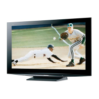
Do you have a question about the Panasonic TH-50PE8U and is the answer not in the manual?
General repair guidelines and specific leakage current test procedures for safety.
Techniques to minimize component damage from electrostatic discharge during handling.
Information on lead-free solder, its melting point, and handling precautions.
Hints for accessing service information and a list of board names and their functions.
Details compatible input signals for Component (Y, PB, PR) and HDMI.
Details on power, display, sound, dimensions, and operating conditions of the TV.
Guides on how to enter service mode and use key commands for navigation and adjustment.
Details the adjustable parameters available within the service mode.
Simple procedure to exit the service mode by turning off the unit.
Instructions to access service tool mode, interpret SOS history, and view power on time.
Details the purpose, access commands, and configuration options for hotel mode.
Procedures for accessing, viewing screen display, and checking points for IIC bus lines.
Guide to identifying defective blocks based on the number of power LED blinks.
Identifies states of 'No Power' indication by power LED and initial checks.
Flowchart to diagnose issues causing the TV to have no picture.
Explains local area failures on the plasma display and identifies defective PCBs.
Step-by-step instructions for removing the back cover, rear terminal cover, and main boards.
Instructions for removing SU, SD, and SC boards from the chassis.
Instructions for removing SS2, SS3, and SS boards from the chassis.
Steps for removing the left and right stand brackets.
Instructions for removing C1, C2, C3, Front bracket, G, and GS boards.
Instructions for removing speakers and the plasma panel assembly from the cabinet.
Procedures for removing S and K boards, and replacing the plasma panel.
Preparation and adjustment steps for driver section voltages, referring to panel data.
Procedure for adjusting initialization pulse and quick adjustments after PCB replacement.
Diagrams showing the locations of adjustment volumes and test points for calibration.
Detailed procedure for adjusting white balance for different color temperatures (Cool, Normal, Warm).
A block diagram illustrating the main functional units and their interconnections.
Block diagram detailing the main block, including tuner side, and the power supply unit.
Block diagram illustrating the digital signal processor, video interface, and audio processing.
Block diagram showing signal processing, control logic, and interface circuits.
Block diagram illustrating plasma panel connections and drive circuits.
Important cautions for cable assembly and wiring diagrams for internal connections.
Visual illustrations of specific cable connections within the unit.
Explains resistor, capacitor, coil, test points, earth symbols, and voltage measurement conventions.
Schematic diagram of the P-Board, covering power supply and PFC sections.
Schematic diagram of the P-Board, detailing power control and voltage regulation circuits.
Schematic diagram of the P-Board, showing power factor correction and voltage conversion circuits.
Schematic diagram of the P-Board, illustrating DC-DC converter and voltage control circuits.
Schematic diagram of the P-Board, detailing power MCU and related circuits.
Schematic diagram of the P-Board, showing DC-DC converters and connections to other boards.
Schematic diagrams for the G, GS, K, and S boards, detailing their respective circuits.
Schematic of the A-Board, focusing on CPU, memory interfaces, and clock generation.
Schematic of the A-Board, detailing DDR memory interface and related components.
Schematic of the A-Board, covering NAND flash, boot ROM, and SD card interface.
Schematic of the A-Board, detailing power supply circuits and DC-DC converters.
Schematic of the A-Board, illustrating video input and audio switching circuits.
Schematic of the A-Board, showing sound processor, audio amplifier, and drive ICs.
Schematic of the A-Board, detailing GenX EEPROM and IIC bus interfaces.
Schematic of the A-Board, illustrating HDMI multiplexer and interface circuits.
Schematic of the A-Board, showing HDMI multiplexer and signal routing.
Schematic of the A-Board, detailing tuner interface and front-end processor.
Schematic of the A-Board, showing IIC bus control and various interface signals.
Schematic of the A-Board, detailing power supply control and DC-DC converters.
Schematic of the A-Board, illustrating FPGA and interface logic.
Schematic of the A-Board, showing front panel interface and DDR memory signals.
Schematic of the A-Board, detailing DDR memory interface and connections to other boards.
Schematic of the C1-Board, showing connections to drivers and panel data.
Schematic of the C1-Board, detailing driver IC connections and panel data interfaces.
Schematic of the C2-Board, showing connections to drivers and panel data.
Schematic of the C2-Board, detailing driver IC connections and panel data interfaces.
Schematic of the C3-Board, showing connections to drivers and panel data.
Schematic of the C3-Board, detailing driver IC connections and panel data interfaces.
Schematic of the SC-Board, illustrating driver ICs and power supply connections.
Schematic of the SC-Board, showing driver ICs and power factor correction circuits.
Schematic of the SC-Board, detailing driver ICs and recovery circuits.
Schematic of the SU-Board, showing driver ICs and connections to panel electrodes.
Schematic of the SU-Board, illustrating driver IC connections and panel electrode interfaces.
Schematic of the SD-Board, showing driver ICs and connections to panel electrodes.
Schematic of the SD-Board, detailing driver IC connections and panel electrode interfaces.
Schematic of the SS-Board, showing driver ICs and power supply circuits.
Schematic diagrams for SS, SS2, and SS3 boards, illustrating driver ICs and power supply.
Shows the component placement and routing on the foil side of the P-Board.
Lists the locations of ICs, transistors, and resistors on both foil and component sides of the P-Board.
Visual layout diagrams for the G, GS, K, and S boards, showing component placement.
Shows component placement and routing on the foil side of the A-Board.
Lists the locations of ICs, transistors, and test points on both sides of the A-Board.
Shows component placement and connector locations on the C1-Board.
Shows component placement and connector locations on the C2-Board.
Shows component placement and connector locations on the C3-Board.
Shows component placement and connector locations on the SC-Board.
Lists the locations of ICs, transistors, and test points on both sides of the SC-Board.
Shows component placement and connector locations on the SU-Board.
Shows component placement and connector locations on the SD-Board.
Shows component placement and connector locations on the SS-Board.
Shows component placement and connector locations on the SS2 and SS3 boards.
Visual exploded view of the TV's mechanical components and their assembly.
A detailed list of mechanical replacement parts, including part numbers and descriptions.
A list of electrical components with part numbers, descriptions, and remarks.
| Screen Size | 50 inches |
|---|---|
| Display Type | Plasma |
| Resolution | 1366 x 768 |
| Aspect Ratio | 16:9 |
| HDMI Ports | 2 |
| Component Video Inputs | 2 |
| Composite Video Inputs | 1 |
| S-Video Input | 1 |
| PC Input | 1 |
| Viewing Angle | 160 degrees |
| RF Input | 1 |
| Audio Output | 20W (10W x 2) |
| Speakers | 2 |