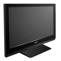
Do you have a question about the Panasonic TH-50PZ80U and is the answer not in the manual?
Guidelines for repairs, modifications, lead dress, and connector handling.
Procedure to measure leakage current in a cold state by checking resistance.
Procedure to check leakage current in a hot state using specific test components.
Techniques to reduce component damage from electrostatic discharge (ESD).
Hints for servicing, including rear cover removal and board identification.
Lists applicable input signals for Component and HDMI, including frequencies.
Details power, display, sound, operating conditions, and connection terminals.
Instructions for accessing Service Mode using button combinations and key commands.
Accessing and using service tool mode for SOS history and power on time.
Restricting functions for hotel use, including access command and menu explanation.
Procedures to access and exit IIC bus line checks via self-check function.
Explains LED blinking patterns to identify defective blocks.
Identifies check points for No Power indication based on power LED status.
Troubleshooting flowchart for diagnosing No Picture issues.
Steps to remove the rear cover and fan unit from the chassis.
Instructions for removing PB-Board, P(AC)-Board, and P(MAIN)-Board.
Steps for removing the P(MAIN)-Board, including cautionary notes.
Steps for removing the plasma panel section from the cabinet assembly.
Details driver set-up and voltage adjustments referring to panel data.
Procedure for adjusting initialization pulse using an oscilloscope.
Detailed procedure for adjusting white balance using a color analyzer.
Overall system block diagram, part 1 of 6, showing major functional units.
Cautions regarding correct assembly and verification of flexible cables.
Diagrams illustrating wiring connections between various boards and components.
Important safety notices and definitions for understanding schematic diagrams.
Detailed schematic diagram for the P(AC)-Board.
Detailed schematic diagram for the P(MAIN)-Board.
Detailed schematic diagram for the A-Board, part 1 of 12.
Detailed schematic diagram for the D-Board, part 1 of 6.
Detailed schematic diagram for the C1-Board, part 1 of 2.
Detailed schematic diagram for the C2-Board, part 1 of 2.
Detailed schematic diagram for the C3-Board, part 1 of 2.
Detailed schematic diagram for the SC-Board, part 1 of 3.
Detailed schematic diagram for the SU-Board, part 1 of 3.
Detailed schematic diagram for the SD-Board, part 1 of 3.
Detailed schematic diagram for the SS-Board, part 1 of 2.
Printed circuit board layout for the P(AC)-Board (Foil and Component sides).
Printed circuit board layout for the P(MAIN)-Board (Foil and Component sides).
Layouts for G, GH, GS, K, and S-Boards (Foil and Component sides).
Layouts for K, PB, S, and SS2-Boards (Foil and Component sides).
Printed circuit board layout for the A-Board (Foil side).
Printed circuit board layout for the D-Board (Foil side).
Printed circuit board layouts for C1-Board (Foil and Component sides).
Printed circuit board layouts for C2-Board (Foil and Component sides).
Printed circuit board layouts for C3-Board (Foil and Component sides).
Printed circuit board layout for the SC-Board (Foil side).
Printed circuit board layouts for SU-Board (Foil and Component sides).
Printed circuit board layouts for SD-Board (Foil and Component sides).
Printed circuit board layouts for SS-Board (Foil and Component sides).
Visual representation of TV assembly with numbered parts for identification.
Detailed list of mechanical parts with part numbers, descriptions, and quantities.
Comprehensive list of electrical components with part numbers and specifications.