

A
Amanda ColeAug 7, 2025
What to do if there is a power supply abnormality in Panasonic Monitor?
- EEric RogersAug 7, 2025
If you encounter a 'Power Supply abnormality' with your Panasonic Monitor, it is recommended to check the P Board (Power SOS).
What to do if there is a power supply abnormality in Panasonic Monitor?
If you encounter a 'Power Supply abnormality' with your Panasonic Monitor, it is recommended to check the P Board (Power SOS).
What should I do if my Panasonic Monitor has a 3.3V line abnormality?
If you are experiencing a '3.3V line abnormality' on your Panasonic Monitor, check the D Board (3.3V SOS).
What to do if a Panasonic Monitor shows Panel Status abnormality?
If there is a 'Panel Status abnormality' with your Panasonic Monitor, check the D, DG Board (Panel Status DET).
Specifies the AC power input requirements for the unit.
Details the maximum and standby power consumption levels.
Technical specifications of the plasma display panel.
Details speaker specifications and audio output power.
Specifies supported PC input signals and scanning frequencies.
Lists the supported channel ranges for digital and analog inputs.
Specifies the recommended temperature and humidity ranges for operation.
Details the types and specifications of input/output connection terminals.
General safety rules and procedures to follow during servicing.
Procedure for checking leakage current when the unit is unplugged.
Procedure for checking leakage current when the unit is powered on.
Methods to reduce component damage from static discharge.
Critical safety notice regarding critical components and modification.
Details on the Sn+Ag+Cu solder used in manufacturing.
Warnings and recommendations for working with lead-free solder.
Recommendations for purchasing Pb free solder.
Diagram showing the physical location of key boards within the unit.
List of main boards and their primary functions.
Step-by-step instructions for removing the back cover of the unit.
Procedure to safely remove the cooling fan.
Instructions for removing the left speaker box assembly.
Instructions for removing the right speaker box assembly.
Procedure to remove the rear terminal cover.
Detailed steps for removing the P-Board and associated components.
Step-by-step procedure for removing the PA-Board.
Instructions for removing the tuner unit from the chassis.
Detailed steps for removing the DT-Board.
Instructions for removing the DG-Board.
Step-by-step guide for removing the H-Board.
Procedure for removing the HC-Board.
Instructions for removing the D-Board.
Steps for removing the SU-Board.
Procedure to remove the SD-Board.
Detailed instructions for removing the SC-Board.
Steps for removing the SS2-Board.
Procedure for removing the SS3-Board.
Instructions for removing the SS-Board.
Steps for removing the C1-Board.
Procedure for removing the C2-Board.
Detailed instructions for removing the C3-Board.
Instructions for removing the stand brackets and rear mounting metals.
Steps for removing the C4-Board.
Procedure for removing the C5-Board.
Instructions for removing the C6-Board.
Steps for removing the front bracket.
Procedure for removing the G-Board and GK-Board.
Instructions for removing the S-Board.
Steps for removing the GS-Board.
Detailed procedure for removing the plasma panel section from the front frame.
Instructions for removing the squawker speaker.
Steps for removing the K-Board.
Final steps for replacing the plasma panel and reassembling the unit.
General caution statement and verification for flexible cables.
Wiring diagram for lead (1)-1.
Wiring diagram for lead (1)-2.
Wiring diagram for lead (2)-1.
Wiring diagram for lead (2)-2.
Procedure to access the self-check function.
Method for exiting the self-check function.
Explanation of the self-check screen output and its interpretation.
Confirmation points for parts if NG (Not Good) is displayed.
Chart detailing Power LED blinking patterns and corresponding defective blocks.
Troubleshooting flowchart for scenarios with no power indication.
Troubleshooting flowchart for scenarios with no picture displayed.
Identification of possible defective PCBs for local screen failures.
Step-by-step guide to access the Serviceman Mode.
Explanation of the key commands for navigating Serviceman Mode.
Method to exit Serviceman Mode.
Details on adjustment modes, values, and sample data.
Procedure to access and use the Memory edit mode.
Procedure to access and interpret Device data mode.
Preparation and procedure for setting up the drivers.
Table and notes for adjusting driver section voltages.
Procedure for adjusting the initialization pulse using an oscilloscope.
Procedure for replacing PCBs and performing quick voltage adjustments.
Diagram showing the location of adjustment potentiometers.
Diagram indicating the location of test points for adjustment.
Detailed procedure for adjusting white balance settings.
Procedure for adjusting sub bright levels using EEPROM addresses.
Procedure for adjusting the Automatic Brightness Limiter (ABL) operation level.
Explanation of the hotel mode's function to restrict features.
Instructions to enter the hotel mode setup menu.
Procedure for exiting the hotel mode setup menu.
Detailed explanation of the hotel mode setup menu items.
Conductor view of the P-Board (foil side).
Conductor view of the PA-Board (foil side).
Conductor view of the H-Board (foil side).
Conductor views and parts locations for G and GS-Boards.
Conductor views and parts locations for GK, HC, K, and S-Boards.
Conductor view of the DG-Board (foil side).
Conductor view of the DT-Board (foil side).
Conductor view of the D-Board (foil side).
Conductor views for the C1-Board.
Conductor views for the C2-Board.
Conductor views for the C3-Board.
Conductor views for the C4-Board.
Conductor views for the C5-Board.
Conductor views for the C6-Board.
Conductor view of the SC-Board (foil side).
Conductor views for the SU-Board.
Conductor views for the SD-Board.
Conductor view of the SS-Board (foil side).
Conductor views for the SS2-Board and SS3-Board.
Notes and symbols used in schematic diagrams.
Overall block diagram of the television system.
Block diagram of the P-Board.
Schematic diagram of the P-Board, part 1 of 3.
Schematic diagram of the P-Board, part 2 of 3.
Schematic diagram of the P-Board, part 3 of 3.
Block diagram of the PA-Board, part 1 of 2.
Block diagram of the PA-Board, part 2 of 2.
Schematic diagram of the PA-Board, part 1 of 3.
Schematic diagram of the PA-Board, part 2 of 3.
Schematic diagram of the PA-Board, part 3 of 3.
Block diagram of the H-Board.
Schematic diagram of the H-Board, part 1 of 3.
Schematic diagram of the H-Board, part 2 of 3.
Schematic diagram of the H-Board, part 3 of 3.
Block diagrams for G, GK, HC, K, and S-Boards.
Schematic diagram of the G-Board.
Schematic diagrams for GK, HC, K, and S-Boards.
Block diagram of the DG-Board, part 1 of 3.
Block diagram of the DG-Board, part 2 of 3.
Block diagram of the DG-Board, part 3 of 3.
Schematic diagram of the DG-Board, part 1 of 8.
Schematic diagram of the DG-Board, part 2 of 8.
Schematic diagram of the DG-Board, part 3 of 8.
Schematic diagram of the DG-Board, part 4 of 8.
Schematic diagram of the DG-Board, part 5 of 8.
Schematic diagram of the DG-Board, part 6 of 8.
Schematic diagram of the DG-Board, part 7 of 8.
Schematic diagram of the DG-Board, part 8 of 8.
Block diagrams for DT and GS-Boards.
Schematic diagram of the DT-Board, part 1 of 7.
Schematic diagram of the DT-Board, part 2 of 7.
Schematic diagram of the DT-Board, part 3 of 7.
Schematic diagrams for DT-Board (part 4 of 7) and GS-Board.
Schematic diagram of the DT-Board, part 5 of 7.
Schematic diagram of the DT-Board, part 6 of 7.
Schematic diagram of the DT-Board, part 7 of 7.
Block diagram of the D-Board, part 1 of 2.
Block diagram of the D-Board, part 2 of 2.
Schematic diagram of the D-Board, part 1 of 8.
Schematic diagram of the D-Board, part 2 of 8.
Schematic diagram of the D-Board, part 3 of 8.
Schematic diagram of the D-Board, part 4 of 8.
Schematic diagram of the D-Board, part 5 of 8.
Schematic diagram of the D-Board, part 6 of 8.
Schematic diagram of the D-Board, part 7 of 8.
Schematic diagram of the D-Board, part 8 of 8.
Block diagrams illustrating the connections between C1, C2, C5, and C6 boards.
Block diagrams showing the interconnections of C2, C4, C3, and C5 boards.
Schematic diagram of the C1-Board, part 1 of 2.
Schematic diagram of the C1-Board, part 2 of 2.
Schematic diagram of the C2-Board, part 1 of 2.
Schematic diagram of the C2-Board, part 2 of 2.
Schematic diagram of the C3-Board, part 1 of 2.
Schematic diagram of the C3-Board, part 2 of 2.
Schematic diagram of the C4-Board, part 1 of 2.
Schematic diagram of the C4-Board, part 2 of 2.
Schematic diagram of the C5-Board, part 1 of 2.
Schematic diagram of the C5-Board, part 2 of 2.
Schematic diagram of the C6-Board, part 1 of 2.
Schematic diagram of the C6-Board, part 2 of 2.
Block diagrams for SC, SU, and SD-Boards.
Schematic diagram of the SC-Board, part 1 of 2.
Schematic diagram of the SC-Board, part 2 of 2.
Schematic diagram of the SU-Board, part 1 of 2.
Schematic diagram of the SU-Board, part 2 of 2.
Schematic diagram of the SD-Board, part 1 of 2.
Schematic diagram of the SD-Board, part 2 of 2.
Block diagrams for SS, SS2, and SS3-Boards.
Schematic diagrams for SS-Board (part 1 of 2), SS2-Board, and SS3-Board.
Schematic diagram of the SS-Board, part 2 of 2.
Diagram showing the physical location of major components.
Visual representation of how the product is packed for shipping.
List of mechanical replacement parts with part numbers and descriptions.
Notes and abbreviations for the electrical parts list.
Detailed list of electrical replacement parts with part numbers and descriptions.
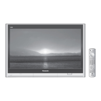
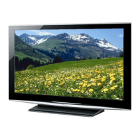
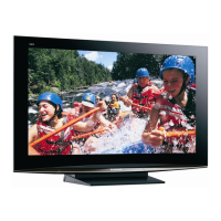
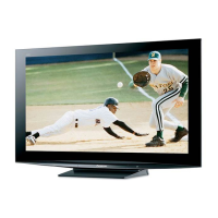
| Screen Size | 58 inches |
|---|---|
| Display Type | Plasma |
| Resolution | 1366 x 768 |
| Aspect Ratio | 16:9 |
| Contrast Ratio | 10000:1 |
| HDMI Ports | 2 |
| Component Video Inputs | 2 |
| Composite Video Inputs | 3 |
| PC Input | Yes |
| HDMI Inputs | 2 |
| Built-in Tuner | ATSC / QAM / NTSC |
| Speaker Output | 20 W (10W x 2) |