6
3 Service Navigation
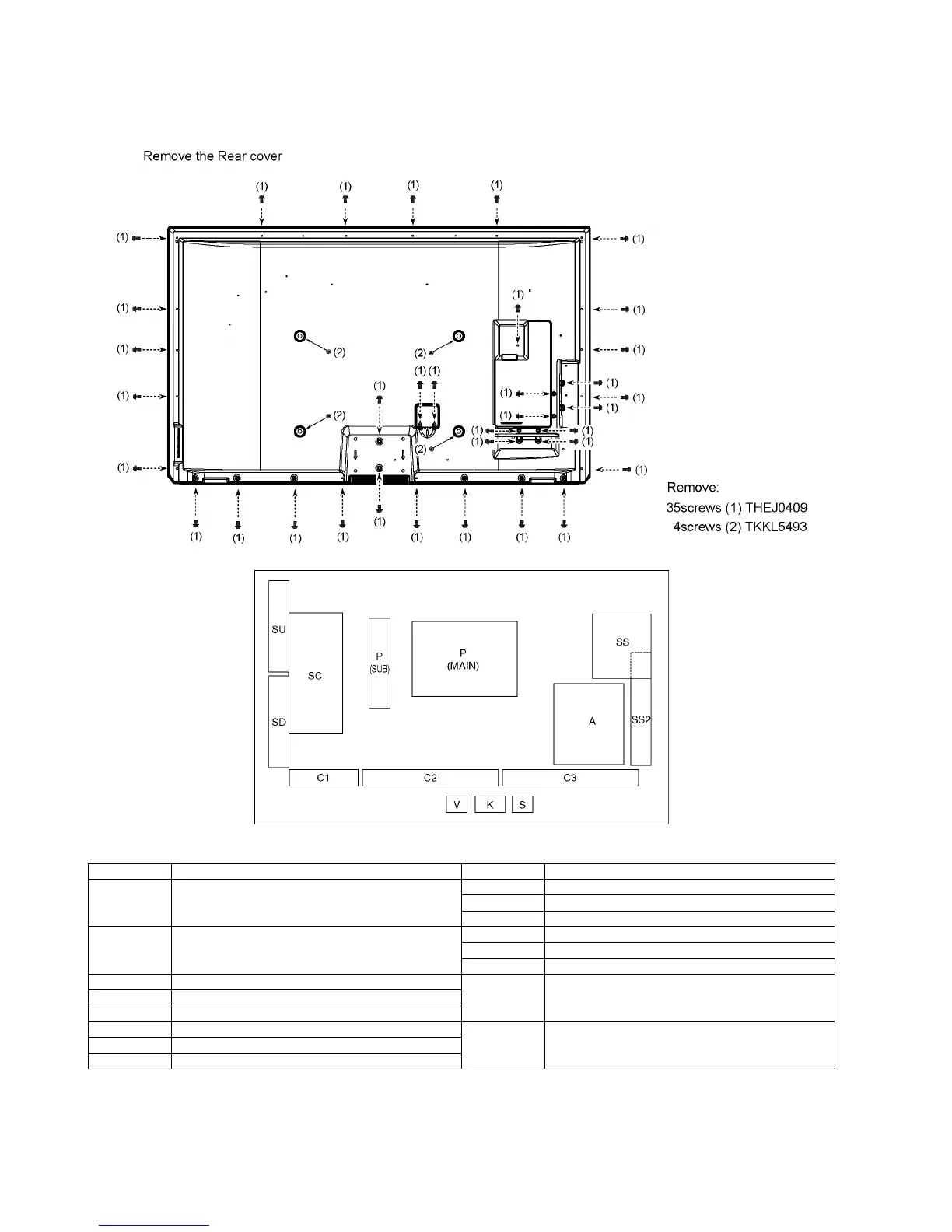
3.1. PCB Layout
Board Name Function Board Name Function
P(MAIN) Power Supply
Non serviceable.
P(MAIN)-Board should be exchange for service.
C1 Data Driver (Lower Right)
C2 Data Driver (Lower Center)
C3 Data Driver (Lower Left)
P(SUB) Power Supply
Non serviceable
P(SUB)-Board should be exchange for service
SC Scan Drive
SS Sustain Drive
SS2 Sustain out (Lower)
A Main AV input, processing SU Scan out (Upper)
Non serviceable.
SU-Board should be exchanged for service.
K Remote receiver, Power LED, C.A.T.S sensor
S Power Switch
V 3D Eyewear transmitter SD Scan out (Lower)
Non serviceable.
SD-Board should be exchanged for service.