Circuit Descriptions
EN 26 TPS14.1A LA7.
2014-Oct-24
back to
div.table
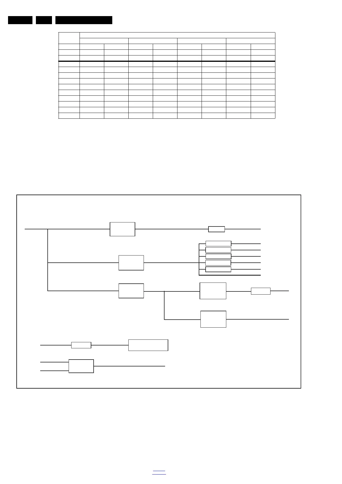
7.3 DC/DC Converters
The on-board DC/DC converters deliver the following voltages
(depending on set execution):
• +5V-STANDBY, permanent voltage for the Stand-by
controller
• +3V3-STANDBY, power supply for LED/IR receiver and
controls
• +12V, input from the power supply for the panel common
(active mode)
• +24V, input from the power supply for the amplifier
• +1V2, from the power supply for the scaler IC MST6931
• +1V8, supply voltage for DDR2 (diagram B03B)
• +3V3, general supply voltage
• +3.3V-TUN, supply voltage for tuner
• +3.3V, supply voltage for Headphone AMP
• +5V-USB, input intermediate supply voltage for USB
Power
• +3V3 from the power supply for the scaler IC MST6931
Figures gives a graphical representation of the DC/DC
converters with its current consumptions:
Figure 7-4 DC/DC converters (for 24PHA4x09)
5 LED3 GND VLED- GND n.c. GND n.c. GND
6 LED4 GND VLED- GND n.c. GND n.c. GND
7 n.c. GND n.c. GND n.c. GND n.c. GND
8 n.c. GND n.c. GND n.c. GND n.c. GND
9 - +12V - +12V_AUDIO VLED_2- +12V_AUDIO VLED_2 +12V_AUDIO
10 - +12V - +12V_AUDIO VLED_2- +12V_AUDIO VLED_2 +12V_AUDIO
11 - +12V - +12V n.c. +12V n.c. +12V
12 - +12V - +12V VLED_2+ +12V VLED+ +12V
13 - +12V - +12V-AL - +12V_AL - +12V
14 - +12V - +12V-AL - +12V-AL - +12V
Connector
24PHA4x09 32PHA4509 40PFA4509 50PFA4509
no. CN8101 CN9904 CN8101 CN9101 CN8101 CN9101 CN8101 CN9301
Descr. to panel to SSB to panel to SSB to panel to SSB to panel to SSB
Pin8 148 1412141214
19660_205.eps
5V_Standby
3.3V_Standby
1.2V_VDDC
+5V_Standby
PANEL_VCC
5V-Normal
FB603
PVDD
P12V
P24V
FB401
VDDC
VDD3.3
AVDD-ADC
AU3.3
FOR SPI Flash
AVDD-DDR
5V-USB
1.8V-DDR
AVDD3.3 DEMOD
VDD3.3-DMPLL
FB408
FB403
FB404
FB405
FB406
FB407
U702
U701
U703
APA2619RI
Q401
A04449
TH701
Q701