Circuit Descriptions, List of Abbreviations, and IC Data Sheets
EN 74 L04E AA9.
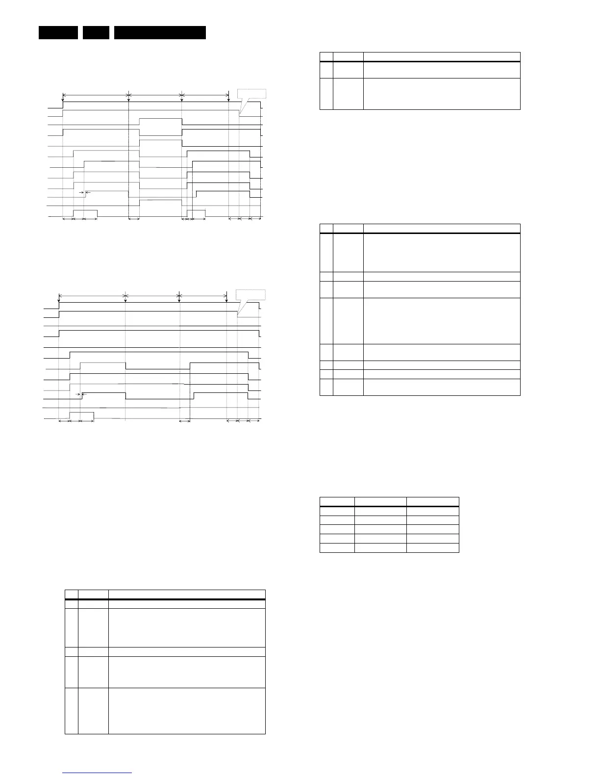
9.2.2 Timing Diagrams
Power ON - To Standby - Out of Standby - Power OFF
Figure 9-2 Timing diagram Standby
Power ON - To Semi Standby - Out of Semi Standby -
Power OFF
Figure 9-3 Timing diagram Semi Standby
9.2.3 Startup Sequence
When the set is connected to the AC power, the rectified line
voltage (via winding 4-5 of L5531 connected to pin 14 of
IC7531) will start the internal voltage source to charge the V_cc
capacitor (C2532). The IC starts to switch as soon as the V_cc
reaches the V_cc start level of 9.5 V. This supply is
automatically taken over by winding 1-2, as soon as the V_cc
is high enough, and the internal supply source will stop (for high
efficiency switching).
Table 9-1 Pinning overview TEA1523
As C2532 of IC7531 is charged, it will also start to charge the
V_cc capacitor (C2511) of IC7511. Via resistor R3519 and
C2511, the TEA1506 starts to switch as soon as the V_cc
voltage reaches the V_cc start level of is about 11 V. The V_cc
voltage is automatically taken over by the main transformer
L5512 (winding 2-3) when the V_cc is high enough (when this
voltage is even higher than the voltage on C2511, there is no
current flow from C2532 to C2511 due to diode D6512).
Table 9-2 Pinning overview TEA1506
9.2.4 Standby Mode
In this mode, IC7511 (TEA1506) will be totally disabled. So
there is no voltage on the main transformer output. But IC7531
(TEA1523) will still work and will provide the necessary output
voltages (6V -> 5V, 3.3V, 3V -> 1.8V) to the Hercules (IC7200).
Table 9-3 PSU voltage overview
9.3 Deflection
9.3.1 Synchronization
Before the Hercules (IC7200) can generate horizontal drive
pulses, the +3.3V supply voltages must be present. After the
start up command of the microprocessor (via I2C), the
Hercules outputs the horizontal pulses. These horizontal
pulses begin “initially” with double line frequency and then
change “gradually” to line frequency in order to limit the current
in the line stage (slow-start).
The VDRA and VDRB signals are the balanced output currents
(sawtooth shaped) of the frame oscillator (pins 106 and 107 of
the Hercules). These output signals are balanced, so they are
less sensitive to disturbances.
Pin Symbol Description
2 Gnd This pin is Ground of the IC.
3 V_cc This pin is connected to the supply voltage. An internal current
charges the V_cc capacitor (2532), and the start-up sequence
is initiated when this voltage reaches a level of 9.5 V. Note: The
output power is disabled when the voltage gets below 9 V
(UVLO). Operating range is between 0 to 40 V.
5 RC Frequency setting
6 REG This pin is connected to the feedback loop. The pin contains two
functions: 1) Between 1 to 1.425 V it controls the "on" time. 2)
Above the threshold of 3.5 V, it is possible to initiate "burst
mode" standby.
11 Demag This pin is connected to the V_cc winding of 5531. It has three
functions: 1) During Magnetisation, the input voltage is sensed
to compensate OCP level for OPP. 2) During demagnetisation,
the output voltage is sensed for OVP and 3) A comparator is
used to prevent continuous conduction when output is
overloaded.
200ms 100ms(ref)
800ms
20ms(ref)
3, 3.3, 6V
Vbat, Vaudio
Normal
VT_supply
POWER_DOWN
+5V
STDBY
2s(ref)
1s(ref)
+1V8 EXT.
10ms(ref)
B
Stdby_con
STB bit
10ms(ref
Power ON
PIP Supplies
Out of Standby
200ms
Standby mode
10mS
Power off
Normal
Relay status
Perform hard-reset
To Standby
Closed
Open
2s(ref)
E_14480_073.eps
200204
Power ON
3, 3.3, 6V
Vbat, Vaudio
To Semi Standby Out of Semi Standby
Power OFF
Semi Standby Normal
Stdby_con
Normal
STB bit
VT_supply
+5V
STDBY
+1V8 ext
PIP Supplies
Relay status
Closed
Open
2s(ref)
800ms
1s(ref)
200ms 20ms (ref) 10ms(ref)
10ms(ref)
B
10mS
under start_up
sequence for details.
Perform
Hard-reset
E_14480_074.eps
200204
12 Sense This pin contains three different functions.: 1) Dectection of soft
start, protection levels of 2) OCP, and 3) SWP.
14 Drain This pin is connected to the drain of the switch or center tap of
the transformer. It contains three functions: 1) M-level (mains-
dependent operation-enabling level), 2) Supply for start-up
current, and 3) Valley detection.
Pin Symbol Description
2 Vcc This pin is connected to the supply voltage. When this voltage
is high (Vcc_start level, about 11 V), the IC will start switching.
When the voltage is lower than Vcc_uvlo (about 8.7 V), the IC
will stop switching.Note: This pin is not self supplied by internal
source like in TEA1507
3 Gnd This pin is Ground of the IC.
6 Ctrl This pin is connected to the feedback loop. The pin will control
the "on" time between 1 V to 1.5 V.
7 Demag This pin is connected to the Vcc winding of 5512. It contains
three functions: 1) During magnetisation, the input voltage is
sensed to compensate OCP level for OPP, 2) During
demagnetisation, the output voltage is sensed for OVP and 3)
a comparator is used to prevent continuous conduction when
the output is overloaded.
9 Sense This pin contains three different functions: 1) dectection of soft
start, protection levels of 2) OCP, and 3) SWP.
11 Driver This pin will drive the (MOSFET) switch.
12 HVS This is High Volt Spacer (n.a.)
14 Drain Connected to the Drain of the external MOSFET switch, this is
the input for valley sensing and initial internal supply.
Voltage Normal operation Stdby mode
V_batt 130 - 143 V 0 V
V_audio +/- 15.5 V 0 V
+6V 6 V 6 V
+3V 3 V 3 V
Stdby_con 0 V 3.3 V
Pin Symbol Description
 Loading...