Circuit Descriptions
EN 51Q552.1L LA 7.
2010-Dec-29
back to
div. table
7.2.3 Connector overview
Table 7-1 Connector overview
7.3 DC/DC Converters
The on-board DC/DC converters deliver the following voltages
(depending on set execution):
• +3V3-STANDBY, permanent voltage for the standby
controller, LED/IR receiver and controls; connector 1M95
pin 1
• +12V, input from the power supply for TV550 common
(active mode); connector 1M95 pins 6, 7 and 8
• +24V, input from the power supply for DVB-S2 (in active
mode); connector 1M09 pins 1 and 2
• +1V1, core voltage supply for PNX85500; has to be started
up first and switched “off” last (diagram B03B)
• +1V2, supply voltage for analogue blocks inside
PNX85500
• +1V8, supply voltage for DDR2 (diagram B03B)
• +2V5, supply voltage for analogue blocks inside
PNX85500 (see diagram B03E)
• +3V3, general supply voltage (diagram B03E)
• +5V, supply voltage for USB and CAM (diagram B03E)
• +5V-TUN, supply voltage for tuner (diagram B03E)
• +V-LNB, input voltage for LNB supply IC (item no. 7T50)
• +5V-DVBS, input intermediate supply voltage for DVB-S2
(diagram B08A)
• +3V3-DVBS, clean voltage for silicon tuner and DVB-S2
channel decoder
• +2V5-DVBS, clean voltage for DVB-S2 channel decoder
• +1V-DVBS, core voltage for DVB-S2 channel decoder.
A +12 V under-voltage detector (see diagram B03C) enables
the 12V to 3.3V and 12V to 5V DC/DC converters via the
ENABLE-3V3-5V line, and the 12V to 1.8V DC/DC converter
via the ENABLE-1V8 line. DETECT2 is the signal going to the
standby microcontroller and ENABLE-3V3n is the signal
coming from the standby microcontroller.
Diagram B03D contains the following linear stabilizers:
• +2V5 stabilizer, built around item no. 7UCO
• +5V-TUN stabilizer, built around items no. 7UA6 and 7UA7
• +1V2 stabilizer, built around items no. 7UA3 and 7UA4.
Diagram B08A contains the DVB-S2-related DC/DC
converters and -stabilizers:
• a +24V under-voltage detection circuitry is built around
item no. 7T04
• the switching frequency of the 24 to 14...20V switched
mode converter is 350 kHz (item no. 7T03 and +V-LNB
lines)
• the output signal on the +V-LNB line goes to the LNBH23Q
(item no. 7T50)
• the LNBH23Q (item no. 7T50) sends a feedback signal via
the V0-CNTRL line
• the switching frequency of the +5V-DVBS to +1-DVBS
switched mode converter is 900 kHz (item no. 7T00)
• a delay line for the +2V5-DVBS and +1V-DVBS lines is
created with item no. 3T03 (R=10k) and 2T06 (C=100n)
• a 3.3V to 2.5V linear stabilizer is built around item no. 7T01
• a 5V to 3.3V linear stabilizer is built around item no. 7T02.
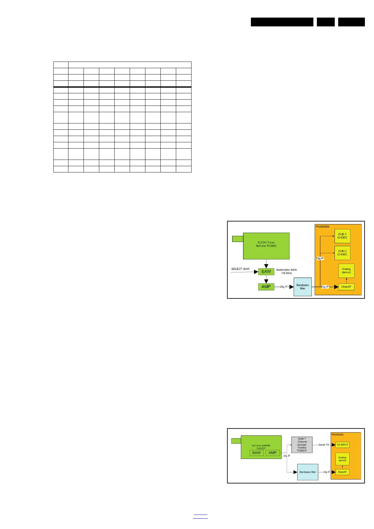
7.4 Front-End Analogue and DVB-T, DVB-C;
ISDB-T reception
7.4.1 European/Asia Pacific region
The Front-End for the European/Asia Pacific region consist of
the following key components:
•Hybrid Tuner
• Switchable SAW filter 7/8 MHz (Eur.), or single SAW filter
(8 MHz) (Asia Pacific)
• Bandpass filter
•Amplifier
• PNX85500 SoC TV processor with integrated DVB-T and
DVB-C channel decoder and analogue demodulator.
Below find a block diagram of the front-end application for this
region.
Figure 7-6 Front-End block diagram European/Asia Pacific region
7.4.2 Latin American region
The Front-End for the Latin American region consist of the
following key components:
• Hybrid Tuner with integrated SAW filter and amplifier
• External ISDB-T channel decoder covering the Brazilian
digital terrestrial TV standard
• Bandpass filter
•Amplifier
• PNX85500 SoC TV with integrated analogue demodulator.
Below find a block diagram of the front-end application for this
region.
Figure 7-7 Front-End block diagram Latin American region
Connector
no. 1308 1311 1319 1316 1M95 1M99 1M09 1MP1
Descr. mains mains disp. disp. to SSB to SSB Amb. T-con
Pin CN1 CN2 CN3 CN4 CN5 CN6 CN7 CN8
1 N L’ t.b.d. t.b.d. 3V3std +12V 24Vb +12V
2 L L” t.b.d. t.b.d. Stndby +12V 24Vb +12V
3 - - - - GND1 GND1 GND1 n.c.
4 - - - - GND1 GND1 GND1 GND1
5----GND1BL_ON
_OFF
- GND1
6----+12VDIM--
7----+12VBoost--
8----+12Vn.c.--
9----+VsndPOK--
10----GND_
SND
---
11----n.c.---
12--------
18770_235_100127.eps
100219
1
8770_236_100127.eps
100219