Do you have a question about the Philips LX8200SA and is the answer not in the manual?
Technical details about power, dimensions, and clock accuracy.
Specifications for audio signal levels, sensitivities, and impedance.
Technical parameters for FM and MW radio reception, including tuning range and sensitivity.
Specifications for various video signal outputs like CVBS, S-Video, and RGB/YUV.
Details on output power, frequency response, and sound modes.
Procedure to verify DVD version matrix and software versions via the remote control.
Procedure for removing key circuit boards from the chassis.
Steps to remove power supply and amplifier components.
Instructions for detaching the front panel unit.
Guide for disassembling control interface components like buttons and LEDs.
Important notes and precautions for servicing the unit, including flex cable handling.
Tests to verify Analog-to-Digital Converter inputs for microprocessors.
Procedures for testing tuner functionality, frequency alignment, and version.
Procedure for testing and formatting the EEPROM for default settings.
Tests related to the DVD module's operation, including version matrix and player functions.
Details on the LCD display unit, its block diagram, and interface pin functions.
Component layout and circuit diagram of the key input board for user controls.
Component layout and circuit diagram for SACD indicator LEDs.
Circuit diagram for volume control and infrared receiver components.
Layout and circuit diagram for the headphone output jack.
Layout and circuit diagram for the power control switch.
Block diagram illustrating the ECO6 Tuner board architecture.
Detailed schematic of the ECO6 Tuner circuitry and component connections.
Table for tuning frequencies, input/output adjustments, and alignment procedures.
Circuit diagram detailing the power supply board's components and connections.
Circuit diagram detailing the main board's circuitry and connections.
Circuit diagram for the power amplifier board, covering input and driver stages.
Circuit diagram for the power amplifier board, covering output stages and protection.
Overview of the AVC board's functions, microprocessor, and key ICs.
Circuit diagram for the AVC board, detailing audio and source selection circuitry.
Circuit diagram for the AVC board, covering digital interfaces and clock/timing circuits.
Circuit diagram for the P-Scan board's line doubler functionality.
Circuit diagram for the P-Scan board's interface and signal processing.
| aspect ratio | 4:3, 16:9 |
|---|---|
| D/A converter (Picture/Display) | 12 bit, 108 MHz |
| D/A converter (Sound) | 24 bit, 192 kHz |
|---|---|
| frequency response | 30-20000 Hz |
| signal to noise ratio | >95 dB |
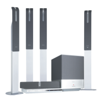
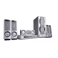
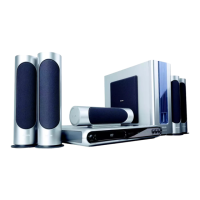
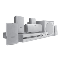
| total sound power (RMS) | 300 W |
| satellite speaker frequency range | 120-50000 Hz |
|---|---|
| satellite speaker impedance | 4 ohm |
| subwoofer frequency range | 30-120 Hz |
| power supply | 200-240 V, 50/60 Hz |
|---|---|
| standby power consumption | < 1 W |
| center speaker dimensions | 286 x 93 x 64 mm |
|---|---|
| subwoofer dimensions | 195 x 460 x 340 mm |
| set dimensions | 390 x 71 x 360 mm |