4.1.4
Frequency display
The circuitry comprises counter and display unit
2
and time base
unit
3.
The signal from the RF generator unit
1
is fed via connection
37
of
unit 6, Schmitt trigger
353,
pre-scale stage
358
and pin 37/~6 to the
counter input 352.12.
The reference frequency for the time base is generated by the X-tal
oscillator in combination with transistor
301.
The
4.000000
MHz
represent the basis wave in parallel resonant circuitry.
Via amplifier 302 the signal is applied to a divider chain. The first
stage
351
serves for division of 1:8, but, if necessary, for quicker
and slower reading of the display, the division can be altered to
1:4
or 1:16 (flickering of the last digit).
Compensating this, the counter
input has either to be applied to
P
or
Q
of unit 6.
The subsequent
integrated circuits 352-355 are switched in for
1
:
lo4
division.
At
solder
joint U
-
suitable for failure chasing
-
50
Hz
(20 ms) can be measured.
Stages 356-358,
361
divide this frequency due to the chosen range in
l(10)-2-5 ratio. The signal, gated by
358,
is applied to the D-flip-flop
359,
generating the ~/2 gate time for the counter decoder driver 352,
unit
2.
Overmore it is applied to double monostable multivibrator
360,
which
generates the store- and reset pulses, determined by the RC combinations
605/514
and 609/516.
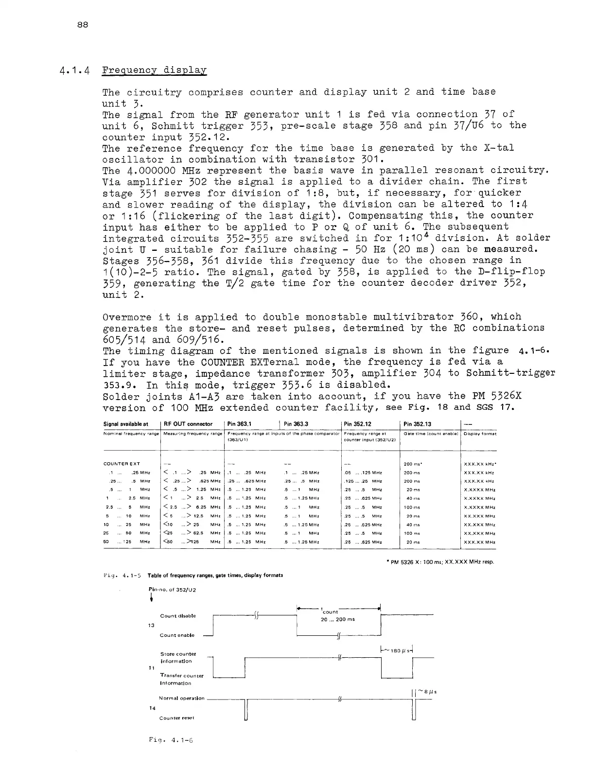
The timing diagram of the mentioned signals is shown in the figure
4.1-6.
If you have the COUNTER EXTernal mode, the frequency is fed via a
limiter stage, impedance transformer
303,
amplifier
304
to Schmitt-trigger
353.9.
In this mode, trigger
353.6
is disabled.
Solder joints
A1-A3
are taken into account,
if you have the
PM
5326X
version of
100
MHz
extended counter facility,
see
Fig.
18
and
SGS
17.
COUNTER
EXT
1
...
.25MHz
25
..
.5 MHz
5
...
1 MHz
1 25 MHz
2.5
...
5 MHz
5
.
10 MHz
10
..
25 MHz
26
..
50 MHz
50
..
125 MHz
--
<
.1
...
>
.25 MHz
<
.25
...
>
,625 MHz
<
.5
...
>
1.25 MHz
<1
..>
25 MHz
<25
..>
625 MHz
<5 .>12.5 MHz
<lo
..>
25 MHz
+5
...
>
62.5 MHz
60 ..A25 MHz
--
D8rpiay format
--
.1
..
.25 MHz
.25
..
,625 MHz
.5
..
1.25 MHz
.5
...
1.25 MHz
.5
.
1.25 MHz
.5 125 MHz
.5
..
1.25 MHz
.5
...
1.25 MHz
.5
...
1.25 MHz
--
.1
...
.25 MHz
.25
..
.5 MHz
.5 .1 MHz
.5 1.25MHz
.5
..
1 MHz
5 1 MHz
.5
...
1.25 MHz
5
...
1 MHz
5
...
1.25 MHz
Pin 363.1
Signal available at
--
05
...
,125 MHz
,125
...
.25 MHz
.25
.
.5 MHz
25
.
625MHz
25
..
5 MHz
.25
. .
5 MHz
.25
..
,625 MHz
.25
...
.5 MHz
.25
...
,625 MHz
Pin 352.13
RF
OUT
connector
Pin 363.3
200
rnr.
200
mr
200
mr
20
mc
do
mr
looms
20
ml
40
rnr
100
mr
20
m3
Gate
time
icount
enable1
Pin 352.12
XXX.XX
kHz.
XXX.XX
kHz
XXX.XX
*HI
X.XXXX
MHz
X.XXXX
MHz
X.XXXX
MHz
XX XXX
MHz
XX.XXX
MHz
XX.XXX
MHz
XXX.XX
MHz
Norntnal
frequency range
PM
5326
X:
100
ms;
XX.XXX
MHz
rerp.
Mearur~ng
frequency
range
Frequency
range
at
inputs
of
the phase comparator
13631U 1
I
Fig.
4.
1-5
Table
of
frequency ranges, gate times, display formats
Frsquency range
at
counter
lnput
13521U2)
Store
counter
Inlormation
11
Transfer
counter
lnformatlan
Normal operation
14
Counter
reset