Circuit Descriptions, Abbreviation List, and IC Data Sheets
EN 126 Q529.1A LA9.
Over-current Detection
Over-current detection is done via components 3U05, 3U06,
3U15, 3U14, and 2U04 for the 3.3 V converter and 3U00, 3U01,
3U16, 3U17, and 2U00 for the 1.2 V converter.
Under-voltage Detection
There is an additional circuit (7U01-1, 7U01-2 and 6U04) to
switch “Off” the 3.3 V converter in case the +12VS drops below
9 V.
Service Tips
• When a power MOS-FET is found defective, replace the
other power MOS-FET as well.
• For a normal operation of the converter, it is important to
check the switching frequency and the value of the boost
voltage.
9.4 Front-End
Refer to figure “9-1 Architecture of TV522/92 platform (AP
region)” earlier in this chapter for details. Refer also to block
diagram B02B.
9.4.1 Device specifications
Tuner (TD1716)
The tuner has the following specifications:
• Hybrid tuner with symmetrical IF output.
• Down conversion from RF to IF frequency (picture carrier
39.875 MHz at analogue reception).
• AGC control signal is coming from master IF device
(TDA9898).
• Only 5 V external supply needed (internal DC-DC
conversion to 3.3 V).
• 4 MHz output is used by master IF device (TDA9898).
The application in this chassis is as follows:
•I
2
C address C0.
• Broadband AGC, no IF section.
•I
2
C communication buffered via MUX.
• Gain to obtain optimised Master IF input level; AGC control
is completely inside the tuner.
• Output level ca. 110 dBμV (for strong input signal).
Repair tip: after replacement of the tuner, the option code
should be checked, even when the set appears to function
correctly! Refer also to chapter 5 “Service Modes, Error Codes,
and Fault Finding”.
Master IF (TDA9898)
• Down conversion from IF to low-IF frequency.
• Down conversion from IF to SIF.
• CVBS output.
The application in this chassis is as follows:
•I
2
C address 0x86.
• Down conversion from IF to low-IF frequency (5.166 MHz
centre frequency).
• Advanced filtering (for further rejection of adjacent
channels).
• Gain to obtain optimised channel decoder level. Control
signal is coming from channel decoder.
SAW filter
X6768 and K9362
• Analogue sound for BG, I, DK, L, L’.
M1973
• Analogue video for BG, I, DK, L, L’.
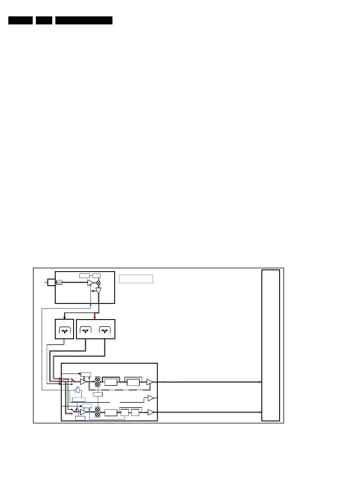
9.4.2 Analogue signal processing (front-end)
Refer to figure “9-5 Analog video broadcast reception block
diagram” for details of analogue signal processing.
Figure 9-5 Analog video broadcast reception block diagram
9.5 PNX85xx
In this chassis, the PNX85xx is responsible for the audio/video
source decode functions and video improvement processing
DVB-T
TDA10048
10-bit
ADC
PLL
Decoding
TS
interface
Tuner
TD1716_Mk4
PLL4MHz
HPF
X6768/K9362
37.67 MHz 38.9 MHz
DVB-C
TDA10023
10-bit
ADC
PLL
Decoding
TS
interface
PNX8541
Side Band
Filter
SIF AGC
Nyquist
Filter
VIF AGC
Band Pass
Filter
Sound
Trap
Group
Delay
TDA9898
PLL
TOP
PEAK AGC
T-AGC
L AGC
338 MHz
M1973
RF
IF
DIF
LIF
SIF
CVBS
TS
IF
IF AGC
RF AGC
Nested AGC
I_17670_007.eps
280408