Page 2.1
VERY HIGH DENSITY MULTIPLEXER CARD 50-670A
pickering
SECTION 2 - TECHNICAL DESCRIPTION
SECTION 2 - TECHNICAL DESCRIPTION
FUNCTIONAL DESCRIPTION
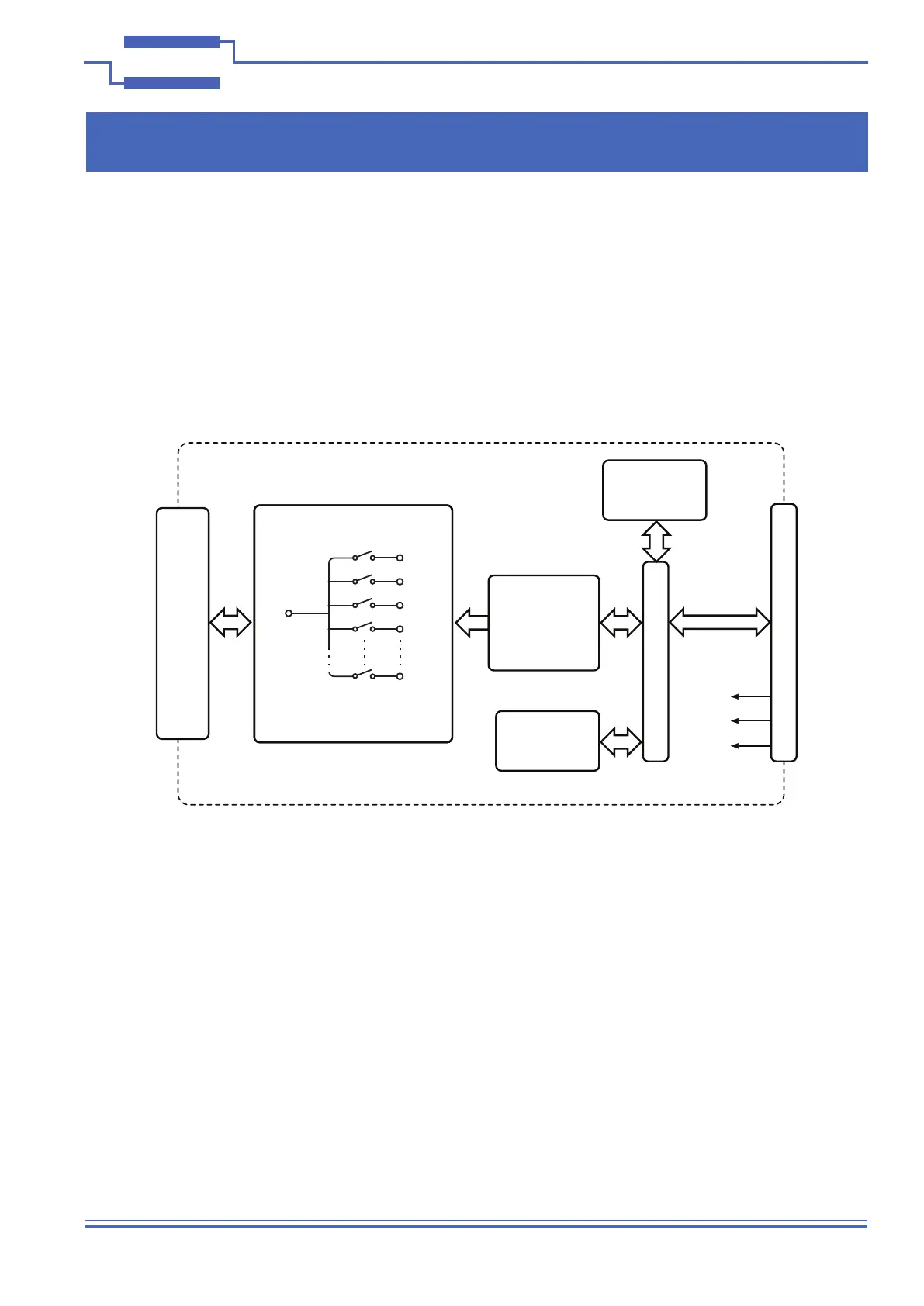
A functional block diagram is provided in Figure 2.1. The Multiplexer Card is powered by +3.3V and +5V inputs via
the PCI edge connector, J2. The interface to the user test equipment is via the front panel mounted 200-pin LFH
connector, J1. The card comprises a PCB populated with up to 101 reed relays. The relays are energised via control
signals from relay drivers U8 to U15. The relay drivers are addressed by PCI bridge U1 to output the required signal.
PCI Bridge U1 is congured by EEPROM U2..
Figure 2.1 - Very High Density Multiplexer Card 50-670A: Functional Block Diagram
Front Panel Connector
200-Pin Female LFH, J1
Relay
Drivers
U8-15
Card
Configuration
U7
PCI Bridge
Configuration
U2
PCI Bridge U1
+3.3V
GND
PCI Bus Edge Connector J2
PCI VERY HIGH DENSITY MUX CARD 50-670A
+5V
Relays RL1-101
One of 11 Different
MUX Configurations


 To Next Page