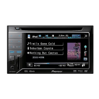
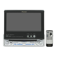
Do you have a question about the Pioneer AVH-P3100DVD/XN/UC and is the answer not in the manual?
| Brand | Pioneer |
|---|---|
| Model | AVH-P3100DVD/XN/UC |
| Category | Car Receiver |
| Language | English |
Order number for the unit.
General warnings for service technicians regarding safe handling and product reliability.
Warning about electrical parts containing chemicals known to cause cancer, birth defects or reproductive harm in California.
Specific safety precautions for servicing, including laser diode handling and distances.
Warning about AEL of laser power output exceeding CLASS 1 limits.
Details on wavelength and focus lens characteristics for CD and DVD.
Caution regarding laser diode activation due to transistor shorts when the top cover is removed.
Warning regarding battery replacement and disposal.
Conforming to regulations, safe servicing environment, and following safety instructions.
Performing optimum adjustments for original product performance according to manual.
Using specified lubricants and adhesives and applying proper amounts.
Proper cleaning procedures for parts like optical pickups, lenses, etc., to restore performance.
Setting shipping mode or installing shipping screws to protect products from transit damage.
General precautions and notes on soldering for safe and proper servicing.
Detailed technical specifications of the product, including general, audio, DVD, and USB features.
Essential checks after servicing, PCB locations, jigs, and cleaning procedures.
Overall connection and block diagrams illustrating system architecture.
Procedures for diagnosing issues, including flowcharts, error codes, and connector functions.
Instructions for accessing and using service modes like monitor test and DVD test modes.
Step-by-step instructions for disassembling the unit and its components.
Procedures for DVD adjustment, monitor unit adjustment, and PCL output confirmation.
Detailed diagrams and lists of parts for packing, exterior components, and the DVD mechanism module.
Circuit diagrams for various PCBs including Mother PCB (Analog, Tuner, System, Power Supply), IF PCB, DVD Core Unit, Connect PCB, and Keyboard PCB.
Connection diagrams for Mother PCB, DVD Core Unit, Connect PCB, IF PCB, Keyboard PCB, and Monitor Unit.
Comprehensive list of electrical components with their part numbers and circuit symbols.
General precautions for servicing, including handling ICs, power, and electrostatic discharge.
Visual guide showing correct and incorrect methods for removing the top case.
Guidelines and recommended lead-free solders for environmental protection and effective soldering.
Detailed technical specifications covering general, audio, display, DVD player, USB, and FM tuner aspects.
Specifications for the AM tuner, including frequency range, usable sensitivity, and signal-to-noise ratio.
Power output and S/N ratio according to CEA2006 standards.
General specifications for AVH-P3100DVD/XN/UC, AVH-P3150DVD/XN/RC, etc., covering audio output and equalizer.
High-pass filter frequency and slope settings, subwoofer frequency and gain settings.
System type, usable discs, region number, supported formats, USB specs, and file system.
Details on MPEG-4 AAC decoding and FM tuner specifications.
Frequency range, sensitivity, S/N ratio for AM tuner, and infrared control specifications.
Visual representation of supported disc formats (CD, DVD) and content types (WMA, MP3, AAC, DivX, JPEG).
Diagram identifying and explaining the function of each button and port on the head unit.
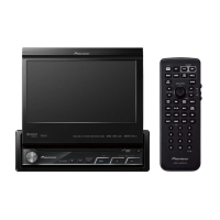
Information about the separately sold remote control and its manual.
Table detailing the button names and their functions in AVH and DVD modes.
Diagram showing the connection of the power cord to the unit, including fuse resistor and ground.
Details on clamping leads and using needle-nosed pliers.
Diagram showing connections for wired remote input, IP-BUS, Bluetooth adapter, and multi-CD player.
Diagram showing connections to power amp via RCA cables and system remote control.
Diagram and warnings regarding rear view camera connection and usage.
Diagram showing connections for multi-channel processor, Bluetooth adapter, and multi-CD player.
Warnings and cautions regarding the installation location and secure fixing of the optical cable connection box.
Instructions for connecting the optical cable and ground lead to the main unit and the connection box.
Diagram showing connections for external video component and display.
Procedures to confirm after servicing to maintain product quality, including customer complaint resolution and media playback checks.
Diagrams showing the physical locations of various PCBs within the unit, including Mother PCB, IF PCB, Keyboard PCB, Monitor Unit, DVD Core Unit, and Connect PCB.
Lists required jigs and their part numbers for LCD, FFC, and PCB connections, as well as discs for skew adjustment and pickup unit inspection.
Lists grease types and their applications for DVD mechanism module and skew adjustment.
Procedures for cleaning DVD pickup lenses and fans before shipping, specifying cleaning tools and materials.
A comprehensive diagram showing the interconnections between major units like Mother PCB, IF PCB, Keyboard PCB, DVD Mechanism Module, and Monitor Unit.
Detailed pinout diagrams for various connectors on the LCD Module, Touch Panel, FM/AM ANT, Power Supply, S/PDIF OUT, and VCR IN.
Detailed block diagram illustrating the functional blocks of the Mother PCB (1/2) and its connections to other units like IF PCB, AV Selector, and IP-BUS Driver.
Detailed block diagram showing the connections within the Mother PCB (2/2), including power connector, amplifier, system uCON, and various ICs and components.
Detailed block diagram for the Mother PCB (2/2), illustrating connections to the FM/AM Tuner Unit, D/D Converter, and various voltage regulators.
Block diagram showing the internal connections of the DVD Core Unit, including Flash ROM, SDRAM, and Motor Driver IC.
Block diagram showing the connections on the Connect PCB, linking to the Spindle Motor and other PCBs.
Diagram illustrating the mechanical unit and its associated components and connectors.
Detailed block diagram of the DVD Core Unit, showing connections to IC1501 (VIDEO+AUDIO MN2DS0018MAUB) and IC1801 (AUDIO 2CH ANALOG OUT PCM1753DBQ).
Block diagram illustrating the connections within the Monitor Unit, including LCD Module, Touch Panel, EEPROM, and various ICs.
Detailed block diagram of the Monitor Unit, showing connections for RGB LED Driver, remote control sensor, and various ports.
Flowchart for diagnosing operational status, including checks for Vdd, BSENS, ASENS, STANDBY, ASENBO, VDCNT, and SYSPW.
Flowchart detailing the inspection process for the pickup unit, including checks for LD, RF level, error rate, and lens cleaning.
Procedures and specifications for checking LD current for DVD and CD discs, including test mode status and expansion views of test points.
Procedures and specifications for checking ASMAX value (RF level) and the sequence of displays during FOCS CLOSE.
Procedures and specifications for checking error rate for DVD and CD discs, including test mode display and connect rear monitor output.
Flowchart for diagnosing issues in the back end section, covering playback start, AVCC5 voltage, VDD5/VCC33/VCC12 voltage, reset status, VSENS, 27 MHz, 48 MHz, SDRAM I/F, audio circuit, video circuit, and flash memory life.
Procedure to check standby voltage at the STANBY test point against DGND1 reference.
Procedure to check VDD5, VCC33, and VCC12 voltages at specified test points against DGND1.
Procedure to check the voltage at the XRES test point against DGND1 reference.
Procedure to check the voltage at the VSENS test point against DGND1 reference.
Outline of clock generation and check method for 27 MHz master crystal oscillator frequency.
Outline of SDRAM I/F capacity and communication, and checks for XCSM, XWE, XCAS, XRAS.
Table detailing conductivity checks for signal names between IC1480 and IC1501.
Diagrams showing check points for SDRAM I/F on Side B and Side A.
Procedure to check VD8, VD, and VCC5 voltages at specified test points against PGND3 and AGND1.
Procedure to check AVCC5 voltage at the stylus against PGND and GNDAU.
Outline of DACCLK creation and check method for IC1501 and IC1801, including specification values.
Diagrams showing check points for 27 MHz and DACCLK on Side A and Side B.
Outline of serial digital output to analog audio signal conversion and check method for ADOUT3, SRCK, LRCK, and analog audio out.
Diagrams showing check points for serial 3 lines (ADOUT, LRCK, SRCK) and analog audio out.
Analog audio out check points and specification values for LO and RO signals, as well as IEC signal.
Diagram showing the digital audio signal (IECOUT) check point.
Outline of composite signal output and checking method using an oscilloscope with GNDV1 as reference.
Diagram showing the video signal check point.
Method for judging flash memory life based on user operation speed and LD energizing time display.
Outline of 48 MHz clock creation and check method for the crystal oscillator and its connection.
Diagram showing the check point for the 48 MHz signal.
Outline of USB data transmission and checks for USB memory and iPod connections, including communication waves.
Diagram showing check points for USB signals (SDATA, SCLOCK, CP_RESET, D+, D-).
Waveforms for CH1:ADOUT3, CH1:SRCK, CH1:LRCK, CH1:LO, CH2:RO, CH1:IECOUT.
Waveforms for CH1:COMPO, USB memory (D+/D-, DGND) waveforms.
Waveforms for iPod D+/D-, DGND, CP_RESET, SDA, and SCL signals.
Table listing error status, OSD codes, UART meanings, disc compatibility, and method of reset for various error conditions.
Explanations of OSD display codes, UART parameters, Content Protection (CPPM, CPRM), and Audio WaterMark (AWM).
Table listing messages, causes, and actions for unplayable files, skipped files, protected files, N/A USB, and check USB issues.
Table listing messages, causes, and actions for communication failures and no songs.
Diagrams and lists of connectors on the rear panel, including Wired Remote Control, Video Input/Output, Rear Camera In, Antenna, Front Output, Audio Input, Optical Output, and IP-BUS Input.
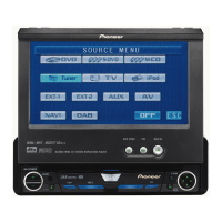
Instructions on how to enter the monitor test mode and its display specifications.
Procedure to access and view version information within the monitor test mode.
Instructions on how to activate and perform touch panel calibration, including menu types and conditions for adjustment completion marks.
Explanation of how to obtain and store outermost circumference values of X and Y, and their allowable ranges.
Description of the 16-point adjustment process, cursor movement, and EEPROM data writing.
Explanation of how coordinate values (Factory, User, Sampling, AD Value, Normalization, Calibration) are displayed and how the cursor can be moved.
Instructions for verifying calibration by touching cursors, with details on correct and incorrect touch feedback.
Explanation of how data initialization returns settings to initial values and writes them to EEPROM.
Instructions on how to enter EEPROM Adjust mode and its display specifications for Flicker Adjust.
Displays related to EEPROM adjustments for LCD protection value, dimmer output, and target arrival time at high temperatures.
Displays related to EEPROM adjustments for common inverted output amplitude, brightness, noise shaping, and RGB gamma correction.
Displays related to EEPROM adjustments for RGB gamma correction and drive adjustments.
Displays related to EEPROM adjustments for horizontal enhancer, YUV DC transmission quantity, and brightness outline correction.
Displays related to EEPROM adjustments for synchronous separation and top curl adjustment under various electric field conditions.
Displays related to EEPROM adjustments for synchronous separation and top curl adjustment under super-weak electric field conditions.
Displays related to EEPROM adjustments for synchronous separation and top curl adjustment under non-signal conditions, and electric field strength judgment values.
Displays related to EEPROM adjustments for color demodulate part (UV delay, phase killer) and AV input picture indication movement.
Describes navigation within the EEPROM adjustment menus.
Instructions on how to enter EEPROM Initialize mode and the process of initializing settings.
Instructions on how to enter Display Test mode and its various test patterns (RGB, Monochrome Stripe, Color Bar).
Display of monochrome stripe signal for flicker adjustment, step signal for alpha blend check, and video signal check.
Explanation of the moving bar signal and its cycle times.
Display of signal for step confirmation, Black/White signal, and screen central location setting.
Image of the test mode and instructions on how to enter it. Legend for key operations and data display.
Flowchart illustrating the front end test mode, including disc type selection, error rate measurement, and LD ON/OFF control.
Flowcharts detailing the procedures for tracking balance, RF level, error rate measurement, and disc selection.
Flowchart for EDC1/2 test mode, including layer selection and ID designation.
Flowchart for LD power on time mode, showing CD and DVD time indication and setting.
Flowcharts for various simple tests including LD ON, ASMAX, Skew Adjustment, Error Rate, CRG Move Outer, and Eject.
Instructions on how to enter and unlock the DVD touch panel test mode, along with its summary and remarks.
Step-by-step instructions and diagrams for removing the unit's case and monitor assembly.
Step-by-step instructions and diagrams for removing the monitor and keyboard PCBs.
Instructions and diagram for removing the DVD mechanism module.
Instructions and diagrams for removing the chassis upper and heat sink.
Instructions and diagrams for removing the mother unit, including straightening tabs and case removal precautions.
Visual guide demonstrating correct (Handling OK) and incorrect (Handling NG) handling procedures for specific parts.
Steps for bringing the mecha module into clamp state with no disc loaded, including FFC removal and applying voltage.
Steps for bringing the CRG mecha into clamp state, including washer and drive gear removal, and clamp arm operation. Includes precautions for installation.
Instructions for removing the module PCB, including shorting FPC spots, removing FFCs, and detaching the PCB.
Step-by-step instructions for removing and installing the relay PCB, including FFC removal, solder removal, and hook alignment.
Steps for removing the pickup unit, including biasing spring hook, sliding, and tucking joints. Includes precautions for installation and sending PU to outer periphery.
Precautions for DVD adjustment, emphasizing correct reference voltage usage (VREF, VHALF) and avoiding grounding contacts. Also includes notes on power OFF procedures and laser diode safety.
When SKEW adjustment is required, measurement equipment, jigs, and bond types used. Includes disc used and symptom for inadequate adjustment.
Explains two methods for adjustment: monitoring RF waves with an oscilloscope (method 1) and checking numerical RF level via OSD (method 2). Details the adjusting procedure, including test mode selection and screw adjustments.
Illustrates the Skew Adjustment screen in TEST MODE, including power OFF and CRG Move Outer selections. Also shows how to produce the clamping state with no disc loaded.
Instructions for CRG Move Outer test, including DVD single layer selection and adhesive application locations.
Instructions for CRG Move Outer test with Power OFF selection.
Instructions for selecting Eject mode within the TEST MODE.
Diagrams showing specific points A and B for SKEW adjustment.
Diagrams illustrating the points for applying adhesive for SKEW adjustment.
Diagram showing the location for applying resonance bond.
Diagrams showing locations for applying screw locking bond.
Shaded areas to avoid touching on the PU, including optical part, RF level adjusting part, and hologram.
Diagram showing the adjustment points on the MONITOR UNIT (SIDE B).
Table detailing adjustment items, input signals, measurement points, specification values, and notes for various voltage and tone voltage checks.
Table detailing further adjustment items, input signals, measurement points, adjustment procedures, and notes for image check and flicker adjustment.
Procedure for confirming PCL output by shifting TESTIN to H and checking the clock signal frequency.
Diagram illustrating the packing contents with numbered parts.
List of parts included in the packing, with part numbers and descriptions.
Table comparing model numbers (AVH-P3100DVD/XN/UC, etc.) and their respective parts (Cover, Unit Box, Owner's Manual, etc.).
Exploded view diagram showing the exterior parts of the unit with numbered components.
Parts list corresponding to the exploded view diagram, with part numbers.
Table comparing model numbers and their specific parts (Grille Unit, Mother Unit, Remote Control Unit, Cover).
Exploded view diagram showing additional exterior parts of the unit with numbered components.
Parts list corresponding to the exterior (2) diagram.
Contrast table comparing parts across different model numbers.
Exploded view diagram of the DVD mechanism module with numbered components and reference labels (A, B, C).
Parts list for the DVD mechanism module, detailing part numbers for screws, washers, springs, levers, gears, motors, connectors, etc.
Diagrams showing component locations or mounting points on the DVD mechanism module, referenced by labels (A, B, C).
Schematic diagram of the Mother PCB (Analog), showing connections to various ICs, connectors, and components.
Schematic diagram of the Mother PCB (Analog), detailing connections to AMP IC, PW CONNECTOR, and MONITOR VBS ADJUST circuitry.
Schematic diagram of the Mother PCB (Tuner), showing connections to the FM/AM Tuner Unit (U401) and related components.
Schematic diagram of the Mother PCB (System), illustrating connections to the Monitor Unit, System MICOM, IP-BUS DRIVER, and various ICs and connectors.
Schematic diagram of the Mother PCB (System), showing interconnections between various buses and ICs.
Schematic diagram illustrating connections from the system MICOM to the IP-BUS driver and USB I/F.
Schematic diagram illustrating connections from the system MICOM to the monitor unit and various ICs.
Schematic diagram illustrating connections from the system MICOM to various ICs, including the IP-BUS driver.
Schematic diagram of the Mother PCB (Power Supply), showing voltage regulators, DC/DC converters, and power supply configurations.
Schematic diagram detailing the power supply circuits, including regulators, converters, and protection components.
Schematic diagram of the IF PCB, showing connections to CN2002, JA2003, JA2001, CN121, and various components.
Schematic diagram of the IF PCB, showing connections to IP BUS, B.CAMERA INPUT, and WIRED REMOTE.
Schematic diagram of the DVD Core Unit, showing connections to IC1501, IC1801, IC1401, IC1402, IC1480, and various connectors.
Schematic diagram illustrating connections for voltage detect, DVD core unit components, and motor driver.
Schematic diagram showing connections for DVD core unit components, voltage detect, and host I/F.
Schematic diagram showing connections for motor driver, DVD core unit components, and power supply.
Schematic diagram illustrating connections for video/audio output, USB clock, and various ICs on the DVD core unit.
Schematic diagram showing connections for FLASH ROM, SD RAM, and other components on the DVD core unit.
Schematic diagram of the Connect PCB, showing connections to HOME sensors, CN701, CN101, and M1/M2 motors.
Schematic diagram of the Keyboard PCB, showing connections to CN3003, CN5004, CN3001, CN3002, JA3001, and various components.
Diagram illustrating the physical layout of buttons and their associated circuitry on the keyboard PCB.
Schematic diagram of the Monitor Unit (uCOM), showing connections to TO TOUCH PANEL, CN5401, CN5001, RGB LED DRIVER, and various ICs.
Schematic diagram illustrating connections within the Monitor Unit, showing Flash ROM, SD RAM, and Backlight Part.
Schematic diagram illustrating connections within the Monitor Unit, showing Flash ROM, SD RAM, and Backlight Part.
Schematic diagram illustrating connections within the Monitor Unit, showing RGB LED DRIVER part and backlighting components.
Schematic diagram illustrating connections within the Monitor Unit, showing the touch panel interface and various ICs.
Schematic diagram illustrating connections within the Monitor Unit, showing the RGB LED DRIVER part and various ICs.
Schematic diagram of the Monitor Unit (MONITOR), showing connections to POWER SUPPLY, C VIDEO, and various ICs.
Schematic diagram detailing the power supply circuits, including regulators, converters, and protection components.
Schematic diagram showing connections from the monitor unit to the LCD module and various ICs.
Schematic diagram illustrating connections from the monitor unit to the LCD module and various ICs.
Schematic diagram illustrating connections from the monitor unit to the LCD module and various ICs.
Schematic diagram illustrating connections from the monitor unit to the LCD module and various ICs.
Oscilloscope waveforms for RF signal (CDRF, DVDRF), TD1 signal (FWD, REV, Multi 32), and VHALF signal.
Oscilloscope waveforms for TD1 signal (Traverse 1001REV, 5001FWD, 5001REV), COP-COM signal, and FD1 signal (Play FD, Focus Jump, Focus Close).
PCB connection diagram for the Mother PCB, showing component layout and connector positions.
PCB connection diagram for the Mother PCB, showing component layout and connector positions.
PCB layout diagram for the Mother PCB, indicating fuse locations and component placement.
PCB layout diagram for the DVD Core Unit, showing component placement and connector locations.
PCB layout diagram for the DVD Core Unit, showing component placement.
PCB layout diagram for the Connect PCB (SIDE A), showing component placement and connector locations (CN701, CN1201).
PCB layout diagram for the Connect PCB (SIDE B), showing component placement and connector locations (CN101).
PCB layout diagrams for the IF PCB (SIDE A and SIDE B), showing component placement and connector locations (CN2001, CN2002, JA2001, JA2002, JA2003, JA2004, CN121).
PCB layout diagrams for the Keyboard PCB (SIDE A and SIDE B), showing component placement and connector locations (CN5004, CN521, CN3003, CN3001).
PCB layout diagram for the Monitor Unit, showing component placement and connector locations (CN6101, CN5701, CN6001).
PCB layout diagram for the Monitor Unit, showing component placement and connector locations (CN5001, CN5004, CN5701, CN6001, CN3003).
PCB layout diagram for the Monitor Unit, showing component placement.
PCB layout diagram for the Monitor Unit, showing component placement.
Note regarding omitted parts, chip components, and safety factor marks. Example of IC 301 location. List of ICs, Transistors, and FETs with symbols and part numbers.
List of Diodes, Transistors, FETs, and ICs with their circuit symbols and part numbers.
List of Resistors with their circuit symbols, part numbers, and locations.
List of Resistors with their circuit symbols, part numbers, and locations.
List of Resistors with their circuit symbols, part numbers, and locations.
List of Resistors with their circuit symbols, part numbers, and locations.
List of Resistors with their circuit symbols, part numbers, and locations.
List of Resistors with their circuit symbols, part numbers, and locations.
List of Resistors with their circuit symbols, part numbers, and locations.
List of Resistors with their circuit symbols, part numbers, and locations.
List of Capacitors with their circuit symbols, part numbers, and locations.
List of Capacitors, ICs, and Inductors with their circuit symbols, part numbers, and locations.
List of Resistors with their circuit symbols, part numbers, and locations.
List of Resistors and Capacitors with their circuit symbols, part numbers, and locations.
List of Switches and Resistors with their circuit symbols and part numbers.
List of miscellaneous parts like Pickup Unit, Motor Unit (LOAD/CRG), and Motor (SPINDLE).