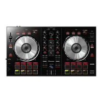

J
Jessica JenkinsAug 2, 2025
How to troubleshoot no sound input/output from USB on Pioneer DJ Equipment?
- KKelsey AdamsAug 2, 2025
If there is no sound input or output from the USB on your Pioneer DJ Equipment, CHECK the Digital Audio Signal Line.
How to troubleshoot no sound input/output from USB on Pioneer DJ Equipment?
If there is no sound input or output from the USB on your Pioneer DJ Equipment, CHECK the Digital Audio Signal Line.
What to do if my Pioneer DDJ-WEGO-K DJ Equipment has a power failure?
If your Pioneer DJ Equipment experiences a power failure, the first step is to CHECK the Power Line.
What to do if there is no sound output from MASTER on my Pioneer DJ Equipment?
If there is no sound output from the MASTER on your Pioneer DJ Equipment, you should: 1. CHECK the Power Line. 2. CHECK the Digital Audio Signal Line. 3. CHECK the Analog Audio Signal Line.
Why is there noise sound output from MASTER on my Pioneer DJ Equipment?
If you are experiencing noise sound output from the MASTER on your Pioneer DJ Equipment, you should: 1. CHECK the Power Line. 2. CHECK the Digital Audio Signal Line. 3. CHECK the Analog Audio Signal Line.
How to fix no sound output from PHONES on Pioneer DDJ-WEGO-K DJ Equipment?
If there is no sound output from the PHONES on your Pioneer DJ Equipment, you should: 1. CHECK the Power Line. 2. CHECK the Digital Audio Signal Line. 3. CHECK the Analog Audio Signal Line.
What causes noise sound output from PHONES on Pioneer DJ Equipment?
If you are experiencing noise sound output from the PHONES on your Pioneer DJ Equipment, you should: 1. CHECK the Power Line. 2. CHECK the Digital Audio Signal Line. 3. CHECK the Analog Audio Signal Line.
What to do if there is no sound input from MIC on my Pioneer DDJ-WEGO-K?
If you're not getting any sound input from the MIC on your Pioneer DJ Equipment, CHECK the Analog Audio Signal Line.
For environmental protection, lead-free solder is used on the printed circuit boards.
On Point-of-Sale Demo Mode. Explains how to enter and exit demo mode.
Recommended check points to confirm product quality after servicing.
Lists required jigs for service, like USB cable.
Illustrates the location of various PCB assemblies within the unit.
Shows the wiring connections between different PCB assemblies.
Illustrates the functional blocks and their interconnections within the unit.
Outlines the step-by-step process the unit follows during startup.
Confirms firmware version and checks user settings like illumination and jog sensitivity.
Verifies proper input and display of buttons, jog dial, and LEDs.
Measures the decline time of the jog dial rotation for diagnosing malfunctions.
Returns user settings to factory defaults and allows for JOG RGB LED color adjustment.
Measures fluctuations in voltage (A/D conversion) for faders and rotary volumes.
Instructions for removing the main chassis section of the unit.
Steps to remove the MASTER and IO PCB assemblies.
Procedures for removing the WHEEL PCB assemblies.
Steps to remove the CONTROL PCB assembly.
Important items to check after repair, including firmware updates.
Detailed procedure for updating the unit's firmware using a PC.
Lists user-configurable settings like jog dial illumination and sensitivity.
Exploded view and parts list for the packing contents.
Detailed schematic diagram for the Control PCB.
Schematic diagrams for the IO and Master PCB assemblies.
Schematic diagrams for the Wheel (R) and Wheel (L) PCB assemblies.
Displays expected waveform patterns for various test points.
Shows the PCB layout and connection points for the Control PCB.
Shows the PCB layout and connection points for the IO PCB.
Shows the PCB layout and connection points for the Master PCB.
Shows the PCB layout and connection points for the Wheel (R) PCB.
Shows the PCB layout and connection points for the Wheel (L) PCB.
| Frequency range | 20 - 20000 Hz |
|---|---|
| Channels quantity | - channels |
| Digital sound processing | - bit |
| Line Signal-to-Noise Ratio (SNR) | 101 dB |
| Total Harmonic Distortion (THD) | 0.006 % |
| Microphone in | Yes |
| Headphone connectivity | 3.5 mm |
| USB 2.0 ports quantity | 1 |
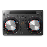
| Product color | Black |
| Apple docking compatibility | iPhone |
| Minimum RAM | 512 MB |
| Minimum processor | Intel Pentium 4/AMD Athlon XP |
| Minimum storage drive space | 50 MB |
| Bundled software | Virtual DJ Limited Edition |
| Depth | 208.5 mm |
|---|---|
| Width | 380 mm |
| Height | 65 mm |
| Weight | 1600 g |