Do you have a question about the Pioneer VSX-516-S and is the answer not in the manual?
Important precautions for safe servicing and product operation, including leakage current checks.
Highlights special safety characteristics of electrical/mechanical parts and the importance of using specified replacement components.
Conformance to regulations, safe servicing environment, proper soldering, screw fastening, and wiring.
Procedures for maintaining original performance and confirming characteristics within specifications.
Guidelines for using correct lubricants, adhesives, and replacement parts for optimal performance.
Proper cleaning procedures for parts like optical pickups and tape heads to restore performance.
Methods to protect products from damage during transit, including setting shipping mode or screws.
Detailed specifications for amplifier power output, input/output sensitivity, frequency response, and tone control.
Specifications for audio input/output, tone control, loudness, signal-to-noise ratio, and crosstalk.
Specifications for video input/output sensitivity, frequency response, and signal-to-noise ratio.
Specifications for component video input/output sensitivity, frequency response, and signal-to-noise ratio.
Specifications for FM tuner frequency range, sensitivity, signal-to-noise ratio, distortion, and selectivity.
Specifications for AM tuner frequency range, sensitivity, and signal-to-noise ratio.
Specifications for power requirements, power consumption, dimensions, and weight.
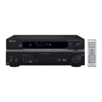
List of parts included with the product, such as antennas, batteries, and remote control.
Exploded view and parts list for the product's packing configuration and included accessories.
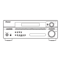
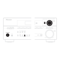
Exploded view of the receiver's exterior parts, showing their locations and part numbers.
Exploded view of the receiver's front panel components, detailing their assembly and part numbers.
High-level functional block diagram illustrating the main signal paths and component interconnections.
Diagram showing the overall wiring connections between various assemblies and connectors in the unit.
Schematic diagram for the first part of the main assembly, detailing its internal circuitry and components.
Schematic diagram for the second part of the main assembly, illustrating its internal circuitry and components.
Schematic diagram for the third part of the main assembly, showing its internal circuitry and components.
Schematic diagram for the first part of the DSP assembly, detailing its digital signal processing circuitry.
Schematic diagram for the second part of the DSP assembly, illustrating its digital signal processing circuitry.
Schematic diagrams for the power pack and transistor assemblies, detailing amplifier and power circuitry.
Schematic diagram for the second part of the power pack assembly, showing its internal circuitry and components.
Schematic diagram for the component assembly, showing its circuitry for video signal routing and control.
Schematic diagrams for the headphone output and 5.1 channel input assemblies, detailing their circuits.
Schematic diagrams for the front display, rotary encoder, and power key assemblies.
Schematic diagrams for transistor and regulator assemblies, showing power supply and voltage regulation circuits.
Schematic diagrams for video, digital input, primary, and transistor 1 assemblies.
Schematic diagram for the USB assembly, detailing its interface and control circuitry.
Schematic diagram for the USB input assembly, showing its connection and signal processing.
PCB layout diagram for the USB input assembly, showing component placement and connector locations.
PCB layout diagram for the main assembly, illustrating component placement and connector locations.
PCB layout diagram for the DSP assembly, showing component placement and connector locations.
PCB layout diagram for the power pack assembly, illustrating component placement and connector locations.
PCB layout diagrams for transistor and power pack assemblies, showing component placement.
PCB layout diagrams for component assemblies, detailing component placement and connector locations.
PCB layout diagrams for headphone and 5.1 channel input assemblies, showing component placement.
PCB layout diagrams for front panel assemblies, illustrating component placement and connector locations.
PCB layout diagrams for regulator and digital input assemblies, showing component placement.
PCB layout diagrams for the video assembly, illustrating component placement and connector locations.
PCB layout diagrams for the primary assembly, showing component placement and connector locations.
PCB layout diagrams for the USB assembly, illustrating component placement and connector locations.
List of all major assemblies with their corresponding part numbers for different models.
Table detailing differences in PCB assemblies and part numbers across various models.
Information related to diagnosing and troubleshooting the unit, including disassembly procedures.
Comprehensive list of parts, including ICs, resistors, capacitors, and connectors, with their respective part numbers.
Detailed explanations of various circuits, protection functions, troubleshooting flowcharts, and module operations.
Diagrams illustrating DC detection, overload detection, fan stop protection, and XPROTECT detection circuits.
Explains the operation of DC abnormality detection, overload detection, and fan stop protection circuits during faults.
Flowchart to diagnose amplifier failures, including checking fan operation, fuses, IC protectors, and supply voltages.
Block diagram of the USB module, showing its main components and connections to the system.
Information on error indications related to USB devices, including overcurrent and unsupported media.
Step-by-step troubleshooting guide for USB connectivity and power supply issues.
Procedures for updating the USB module firmware using a USB memory stick.
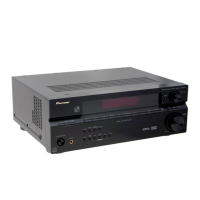
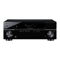
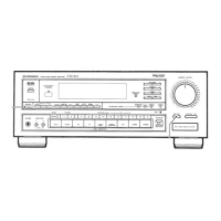
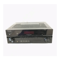
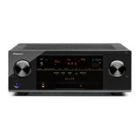
Description and function of the controls and indicators on the front panel of the receiver.
Explanation of the various indicators on the receiver's front panel display and their meanings.
Explanation of the functions of buttons and controls on the remote control unit.
| Input Sensitivity | 200 mV |
|---|---|
| Digital Sound Processor (DSP) | Yes |
| Tuner Bands | AM/FM |
| Power Output (per channel) | 100 W |
| Frequency Response | 10Hz-100kHz |
| Input Impedance | 47 kΩ |
| Tuning Range | FM: 87.5 - 108 MHz, AM: 530 - 1700 kHz |
| Digital Audio Inputs | Optical |