Do you have a question about the Pioneer VSX-519V-K and is the answer not in the manual?
General safety precautions for service technicians and product safety considerations.
Information about special safety characteristics of electrical and mechanical parts.
Ensuring product safety regulations, safe servicing environment, and proper repair procedures.
Guidelines for using lead-free solder and proper soldering techniques for repairs.
Detailed technical specifications for audio, video, tuner, and miscellaneous sections.
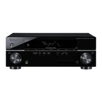
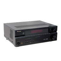
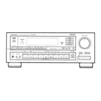
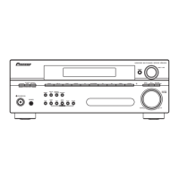
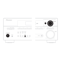
Identification and description of front and rear panel controls and connectors.
Recommended checks to ensure product quality and customer satisfaction after service.
Diagrams showing the physical location of various PCB sub-assemblies within the unit.
List of required jigs for diagnosis and service procedures.
A high-level block diagram illustrating the main component interconnections.
Detailed block diagram of the audio signal path and processing.
Detailed block diagram of the video signal path and processing.
Block diagram showing the microcomputer and control unit connections.
Block diagram illustrating the power supply circuits and voltage distribution.
Step-by-step troubleshooting guide for identifying and resolving product issues.
Circuit diagrams for DC and overload protection detection mechanisms.
How to enter and view protection detection counts (DC, OVERLOAD, TEMP).
Procedure to clear protection detection counts and detailed explanations.
Describes unit behavior and cancellation procedures for DC, OVERLOAD, TEMP errors.
Procedures for safely discharging capacitors on the MAIN and FRONT PCBs.
Critical notes on connecting ground wires during reassembly for safety.
Steps for disassembling and accessing the front panel components.
Procedures for accessing and handling heat sink components.
Steps for removing and accessing the main PCB.
Steps for removing and accessing the DSP PCB.
Procedure for adjusting idle current on the AMP PCB using specified measurement points.
Exploded view and parts list for the product's packing materials.
Exploded view and parts list for external components and chassis.
Schematic diagram for the MAIN and P/T PCB assemblies.
Schematic diagram for the AMP PCB.
Part 1 of the schematic diagram for the DSP PCB.
Connection diagram for MAIN and P/T PCB assemblies.
Connection diagram for the AMP PCB assembly.
List of semiconductor parts with part numbers and locations.
List of miscellaneous parts like coils, tuners, relays, and power transformers.