EasyManua.ls Logo

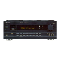
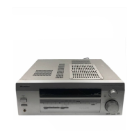
Pioneer VSX-D509S Service Manual

Pioneer VSX-D509S
61 pages
To Next Page IconTo Next Page
Page #1 background imageLoading...
Page #1 background image
ORDER NO.
PIONEER CORPORATION 4-1, Meguro 1-chome, Meguro-ku, Tokyo 153-8654, Japan
PIONEER ELECTRONICS SERVICE, INC. P.O. Box 1760, Long Beach, CA 90801-1760, U.S.A.
PIONEER EUROPE N.V. Haven 1087, Keetberglaan 1, 9120 Melsele, Belgium
PIONEER ELECTRONICS ASIACENTRE PTE. LTD. 253 Alexandra Road, #04-01, Singapore 159936
PIONEER CORPORATION 2000
c
RRV2253
1. SAFETY INFORMATION
......................................
2
2. EXPLODED VIEWS AND PARTS LIST
...............
3
3. BLOCK DIAGRAM AND SCHEMATIC DIAGRAM
.....
8
4. PCB CONNECTION DIAGRAM
.........................
28
5. PCB PARTS LIST
...............................................
43
6. ADJUSTMENT
....................................................
47
CONTENTS
7. GENERAL INFORMATION
................................
48
7.1 DISASSEMBLY
............................................
48
7.2 PARTS
..........................................................
49
7.2.1 IC
............................................................
49
7.2.2 DISPLAY
.................................................
54
8. PANEL FACILITIES AND SPECIFICATIONS
.......
56
T – ZZK JAN. 2000 Printed in Japan
THIS MANUAL IS APPLICABLE TO THE FOLLOWING MODEL(S) AND TYPE(S).
PHONES
MPX
MODE
MIDNIGHT
AUXVIDEO
BASS TREBLE
2
/DTS
SIGNAL
SELECT
1
R
N∫m-Û.?/∫ Digital Signal Processor
S-VIDEO VIDEO L AUDIO R
VIDEO INPUT
AUDIO/VIDEO MULTI-CHANNEL RECEIVER
VSX-D509S
Type
Model
Power Requirement Remarks
VSX-D509S
KUXJI AC120V
KCXJI AC120V

Other manuals for Pioneer VSX-D509S

Question and Answer IconNeed help?

Do you have a question about the Pioneer VSX-D509S and is the answer not in the manual?

Pioneer VSX-D509S Specifications

General IconGeneral
BrandPioneer
ModelVSX-D509S
CategoryReceiver
LanguageEnglish

Summary

1. Safety Information

1. Safety Precautions

Outlines precautions for customer and service technician protection.

Leakage Current Check

Details the procedure and limits for measuring AC leakage current.

2. Product Safety Notice

Highlights safety characteristics of replacement components and potential hazards.

3. Block Diagram and Schematic Diagram

3.1 Block Diagram

Overall functional block diagram showing the signal flow and interconnections between major units.

3.2 Overall Wiring Connection Diagram and AMP INPUT ASSY

Diagram illustrating the wiring connections between various internal assemblies and connectors.

3.3 D.D & Input (1/3) Assy

Schematic diagram for the D.D & Input Assy, showing circuit details.

3.4 D.D & Input Assy (2/3)

Continuation of the D.D & Input Assy schematic, detailing more circuit sections.

3.5 D.D & Input Assy (3/3)

Final part of the D.D & Input Assy schematic, showing remaining circuit details.

3.6 AMP&Primary (1/2), TRANS2 and TRANS3 ASSYS

Schematic diagrams for the Amp&Primary, Trans2, and Trans3 assemblies.

3.7 AMP&Primary (2/2), REGULATOR and TRANS1 ASSYS

Schematic diagrams for Amp&Primary (cont.), Regulator, and Trans1 assemblies.

3.8 VIDEO&6CH IN, H. P. and DIGITAL IN ASSYS

Schematic diagrams for Video&6CH In, H.P., and Digital In assemblies.

4. PCB Connection Diagram

5. PCB Parts List

6. Adjustment

7.2.1 IC

8. Panel Facilities and Specifications

8.2 Specifications

Technical specifications for amplifier, tuners, and other sections of the receiver.

Connecting Audio Components

Related product manuals