Rev. J 08/16
2
TOP252-262
www.power.com
EcoSmart™– Energy Efficient
• Energy efficient over entire load range
• No-load consumption
• Less than 200 mW at 230 VAC
• Standby power for 1 W input
• >600 mW output at 110 VAC input
• >500 mW output at 265 VAC input
Description
TOPSwitch™-HX cost effectively incorporates a 700 V power
MOSFET, high voltage switched current source, PWM control,
oscillator, thermal shutdown circuit, fault protection and other
control circuitry onto a monolithic device.
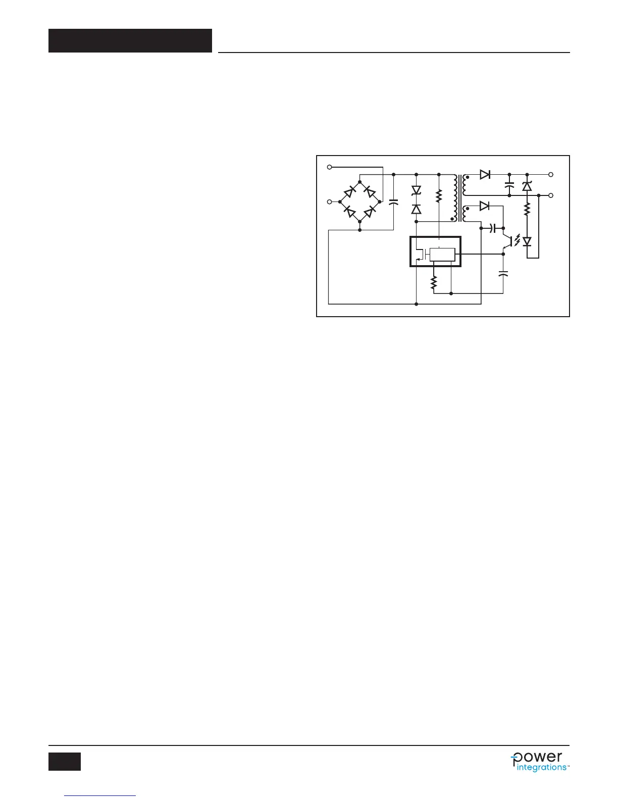
Figure 2. Typical Flyback Application TOP259YN, TOP260YN and TOP261YN.
Y Package Option for TOP259-261
In order to improve noise-immunity on large TOPSwitch-HX
Y package parts, the F pin has been removed (TOP259-261YN
are fixed at 66 kHz switching frequency) and replaced with a
SIGNAL GROUND (G) pin. This pin acts as a low noise path for
the C pin capacitor and the X pin resistor. It is only required for
the TOP259-261YN package parts.
Notes for Table 1:
1. Minimum continuous power in a typical non-ventilated
enclosed adapter measured at +50 °C ambient. Use of an
external heat sink will increase power capability.
2. Minimum continuous power in an open frame design at
+50 °C ambient.
3. Peak power capability in any design at +50 °C ambient.
4. 230 VAC or 110/115 VAC with doubler.
5. Packages: P: DIP-8C, G: SMD-8C, M: SDIP-10C,
Y: TO-220-7C, E: eSIP-7C, L: eSIP-7F.
See part ordering information.
6. TOP261 and TOP262 have the same current limit set point. In
some applications TOP262 may run cooler than TOP261 due
to a lower R
DS(ON)
for the larger device.
PI-4973-122607
AC
IN
DC
OUT
D
S
C
TOPSwitch-HX
CONTROL
V
+
-
GX