Rev. J 08/16
6
TOP252-262
www.power.com
Pin Functional Description
DRAIN (D) Pin:
High-voltage power MOSFET DRAIN pin. The internal start-up
bias current is drawn from this pin through a switched high-
voltage current source. Internal current limit sense point for
drain current.
CONTROL (C) Pin:
Error amplifier and feedback current input pin for duty cycle
control. Internal shunt regulator connection to provide internal
bias current during normal operation. It is also used as the
connection point for the supply bypass and auto-restart/
compensation capacitor.
EXTERNAL CURRENT LIMIT (X) Pin (Y, M, E and L package):
Input pin for external current limit adjustment and remote
ON/OFF. A connection to SOURCE pin disables all functions on
this pin.
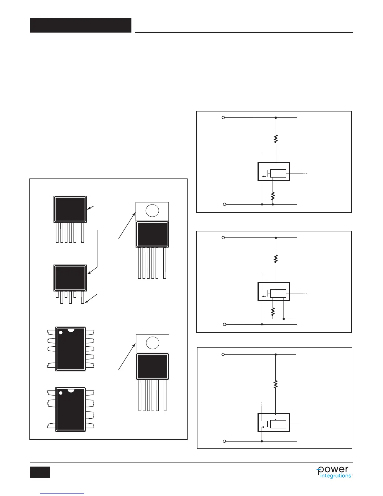
Figure 4. Pin Configuration (Top View).
X
PI-4711-021308
DC
Input
Voltage
+
-
D
S
C
CONTROL
V
R
IL
R
LS
12 kΩ
4 MΩ
V
UV
= I
UV
× R
LS
+
V
V
(I
V
= I
UV
)
V
OV
=
I
OV
×
R
LS
+
V
V
(I
V
= I
OV
)
For R
LS
=
4
MΩ
DC
MAX
@100 VDC = 76%
DC
MAX
@375 VDC = 41%
For R
IL
= 12 kΩ
I
LIMIT
= 61%
See Figure 55b for
other resistor values
(R
IL
) to select different
I
LIMIT
values.
V
UV
= 102.8 VDC
V
OV
= 451 VDC
Figure 5. TOP254-258 Y and All M/E/L Package Line Sense and Externally Set
Current Limit.
PI-4712-120307
DC
Input
Voltage
+
-
D M
S
C
V
UV
= I
UV
× R
LS
+
V
M
(I
M
= I
UV
)
V
OV
=
I
OV
×
R
LS
+
V
M
(I
M
= I
OV
)
For R
LS
= 4 MΩ
V
UV
= 102.8 VDC
V
OV
=
451 VDC
DC
MAX
@100 VDC = 76%
DC
MAX
@375 VDC = 41%
CONTROL
R
LS
4 MΩ
Figure 7. P/G Package Line Sense.
X G
PI-4983-021308
DC
Input
Voltage
+
-
D
S
C
CONTROL
V
R
IL
R
LS
12 kΩ
4 MΩ
V
UV
= I
UV
× R
LS
+
V
V
(I
V
= I
UV
)
V
OV
=
I
OV
×
R
LS
+
V
V
(I
V
= I
OV
)
For R
LS
=
4
MΩ
DC
MAX
@100 VDC = 76%
DC
MAX
@375 VDC = 41%
For R
IL
= 12 kΩ
I
LIMIT
= 61%
See Figure 55b for
other resistor values
(R
IL
) to select different
I
LIMIT
values.
V
UV
= 102.8 VDC
V
OV
= 451 VDC
Figure 6. TOP259-261 Y Package Line Sense and External Current Limit.
VOLTAGE MONITOR (V) Pin (Y & M package only):
Input for OV, UV, line feed forward with DC
MAX
reduction, output
overvoltage protection (OVP), remote ON/OFF and device reset.
A connection to the SOURCE pin disables all functions on this pin.
MULTI-FUNCTION (M) Pin (P & G packages only):
This pin combines the functions of the VOLTAGE MONITOR (V)
and EXTERNAL CURRENT LIMIT (X) pins of the Y package into
one pin. Input pin for OV, UV, line feed forward with DC
MAX
PI-4644-091108
Tab Internally
Connected to
SOURCE Pin
Tab Internally
Connected to
SOURCE Pin
Lead Bend
Outward from Drawing
(Refer to eSIP-7F Package
Outline Drawing)
Exposed Pad
(Hidden)
Internally
Connected to
SOURCE Pin
Y Package (TO-220-7C)
D
C
S
S
S
S
S
S
S
S
S
7
D
5
F
4
S
3
C
2
X
1
V
7
D
5
S
4
F
3
C
2
X
1
V
7
D
5
S
4
F
3
C
2
X
1
V
7
D
5
G
4
S
3
C
2
X
1
V
M
P and G Package
M Package
8
5
7
1
4
2
6
D
X
C
V
10
6
9
1
5
8
7
2
3
Note: Y package for TOP259-261
Note: Y package for TOP254-258
E Package (eSIP-7C)
L Package (eSIP-7F)
Y Package (TO-220-7C)
 Loading...