VIDEO RAM
TROUBLESHOOTING (Continued)
KEYBOARD
The
following
Basic program can be used
to
check
the RAM
ICs (Z45 thru Z48 and
Z61
thru Z63). The program checks
each
bit
of RAM and displays on the
Monitor
screen any
defective
bit
found. If a Printer is connected
to
the Com-
puter,
the
bad
bit
message can be sent
to
the
Printer by
changing the word PRINT in lines 130 and 150
to
the word
LPRINT.
VIDEO RAM TEST PROGRAM
5 DATA
1,
2,
4,8,16,32,128
10
Y =
6:
X = 15360: POKE
X,64
20
IF (PEEK
(X)
AN
0
64)
=
64
TH
EN
30
ELSE 150
30
POKE X,160
40
IF (PEEK
(X)
AND
64)
= 0 THEN
50
ELSE 150
50
FOR X = 15360 TO 16383
60
FOR
Y=O
TO
6
70
READ
Z:
POKE X,Z
80 IF (PEEK
(X)
AND
Z)
= Z THEN 90 ELSE 140
90 POKE
X,O
100
IF (PEEK
(X)
AND
Z)=O
THEN 110 ELSE 140
110 NEXT Y
120 RESTORE: NEXT X
130 PRINT "MEMORY GOOD" : END
140
IF Y = 6
TH
EN
Y = 7
150
PRINT
"BIT";
Y;
"OF
MEMORY LOCATION";
X;
"CHECKS BAD"
160
IF Y = 6 THEN 50 ELSE 110
Keyboard is
not
functioning.
Check the ribbon cable be·
tween Keyboard and
CPU
Board
for
open
circuits.
If the rib-
bon cable checks good, check
for
pulses at pin
11
of
IC Z36.
If pulses are
missing,
check IC Z36 by
substitution.
If a
group
of
keys are
not
functioning,
check the pins of ICs
Z1A and Z2A and Tri-State Inverter ICs (Z3A and Z4A) con-
nected
to
the keys
not
functioning.
Also
check the ribbon
cable
for
open
circuits.
If
a single key does
not
function,
check the key
contacts
with
an
ohmmeter. If the key is erratic and
intermittent
in
operation, clean the
contacts
with
a spray
contact
cleaner.
If a wrong character shows up on the
Monitor
screen when
an alpha or numeric key is pressed, check the video RAM,
refer
to
the
"Video
RAM"
section
of
this
Troubleshooting
guide
and check Flip/Flop IC
(Z28)
and Character Generator
IC
(Z29)
by
substitution.
CASSETIE
Computer
will
not
save programs
onto
tape or
will
not
turn
On the cassette motor. Type and run the
following
Basic
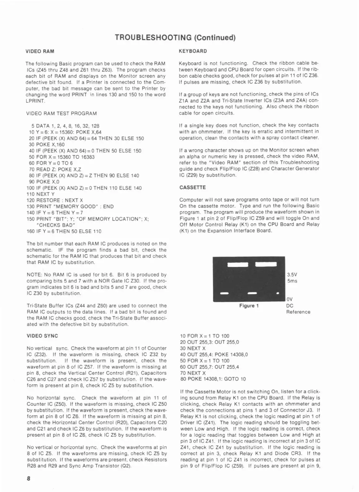
program. The program will produce the waveform shown in
Figure 1 at pin 2
of
Flip/Flop IC Z59 and
will
toggle
On and
Off
Motor
Control Relay (K1) on the
CPU
Board and Relay
(K1) on the Expansion Interface Board.
The
bit
number
that each RAM IC produces is noted on the
schematic. IF the program finds a bad bit, check the
schematic
for
the RAM IC that produces that
bit
and check
that RAM IC by
substitution.
NOTE:
No
RAM IC is used
for
bit
6.
Bit 6 is produced by
comparing
bits
5 and 7
with
a NOR Gate IC Z30. If
the
pro-
gram
indicates
bit
6 is bad and
bits
5 and 7 are good, check
IC
Z30 by
substitution.
Tri-State
Buffer
ICs
(Z44
and Z60) are used
to
connect
the
RAM IC
outputs
to the data lines. If a bad
bit
is found and
the RAM IC checks good, check the Tri-State
Buffer
associ-
ated
with
the defective
bit
by
substitution.
Figure 1
3.5V
5ms
OV
DC
Reference
VIDEO SYNC
No vertical sync. Check the waveform at pin
11
of
Counter
IC
(Z32).
If
the
waveform is missing, check IC Z32 by
substitution.
If
the
waveform is present, check the
waveform at pin 8 of IC Z57. If the waveform is
missing
at
pin
8,
check
the
Vertical Center Control
(R21),
Capacitors
C26
and C27 and check IC Z57 by
substitution.
If the wave-
form is present at pin
8,
check IC Z5 by
substitution.
No horizontal sync. Check the waveform at pin
11
of
Counter IC
(Z50).
If the waveform is
missing,
check IC Z50
by
substitution.
If the waveform is present, check the wave·
form at pin 8
of
IC Z6.
If
the waveform is
missing
at pin
8,
check the Horizontal Center Control
(R20),
Capacitors C20
and
C21
and check IC
Z6
by
substitution.
If
the waveform is
present at pin 8 of IC
Z6,
check IC
Z5
by
substitution.
No vertical or horizontal sync. Check the waveforms at pin
8
of
IC Z5. If the waveforms are missing, check IC
Z5
by
substitution.
If the waveforms are present, check Resistors
R28
and
R29
and Sync Amp
Transistor
(02).
8
10
FOR
X=
1
TO
100
20
OUT 255,3: OUT 255,0
30
NEXT X
40
OUT 255,4: POKE 14308,0
50
FOR
X=
1
TO
100
60
OUT 255,7: OUT 255,4
70
NEXT X
80
POKE 14308,1: GOTO
10
If
the
Cassette
Motor
is not
switching
On, listen
for
a
click·
ing sound from Relay
K1
on the
CPU
Board. If the Relay is
clicking,
check Relay
K1
contacts
with
an
ohmmeter
and
check
the
connections
at pins 1 and 3
of
Connector
J3. If
Relay
K1
is
not
clicking,
check the
logic
reading at pin 1 of
Driver IC
(Z41).
The
logic
reading should be
toggling
bet-
ween Low and High. If the
logic
reading is correct, check
for
a
logic
reading that toggles between Low and High at
pin 3 of IC Z41. If the
logic
reading is incorrect at pin 3
of
IC
Z41, check IC
Z41
by
substitution.
If the
logic
reading is
correct
at pin
3,
check Relay
K1
and Diode CR3. If the
reading at pin 1
of
IC
Z41
is incorrect, check
for
pulses at
pin 9
of
Flip/Flop IC
(Z59).
If pulses are present at pin
9,
 Loading...