Do you have a question about the Samsung HPS5053X/XAA (HP-S5053) and is the answer not in the manual?
Safety precautions for handling the TV, including electrical shock and radiation risks.
Precautions to be followed by service personnel during repairs, including ESD and capacitor handling.
Precautions to prevent damage to static-sensitive devices (ESD) during handling and soldering.
Safety precautions for installing the product, including handling, ventilation, and antenna placement.
Lists the main features of the TV, categorized by block (RF, PDP, Power, Video, Sound, Cabinet).
Details key specifications like model, dimensions, weight, power consumption, pixel count, and input/output terminals.
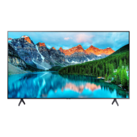
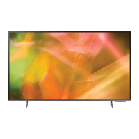
Compares specifications of different models (HP-S5053, HP-P5071, HP-R5072) across various features.
Lists supplied accessories and those that can be purchased additionally, with item codes.
Instructions for service adjustments, including checking items after replacing components like the SMPS or PDP panel.
Step-by-step guide to enter the service mode using the remote control and navigate its menus.
Details factory settings for calibration, option bytes, and white balance adjustments across different input modes.
Detailed procedure for adjusting white balance for CVBS, Component, PC, and HDMI inputs.
Steps for upgrading the TV's software using a USB memory stick.
Procedure for adjusting SMPS panel voltages after replacing SMPS-PCB or PDP module.
Exploded view diagrams and part lists for the HPS5053X/XAA model.
Lists service parts for the HPS5053X/XAA model, including code numbers and specifications.
Initial troubleshooting steps, focusing on cable connections, power input, and board voltages.
Troubleshooting steps for various error modes like No Power, Power Cycling, No Picture, and No Sound.
Lists Assy codes, descriptions, and major symptoms for troubleshooting specific assemblies.
A high-level block diagram illustrating the main components and signal flow of the TV.
Detailed block diagrams for SMPS, DC-DC SMPS, Driver Boards, and Logic Board.
Diagram showing the overall wiring connections between major assemblies like the main board, power, and speakers.
Wiring diagrams illustrating connections between PDP Module/SMPS and Main Board/other boards.
Shows photos and codes for connecting cables like SMPS 12P, LVDS 31P, and POWER 10P.
Diagram showing the layout of components on the PCB and their interconnections.
Schematic diagram of the main power block, detailing power supply circuits and standby power components.
Schematic of the standby MICOM (S3F866B) and its related circuits, including EEPROM and tuner interface.
Schematic of the sound processor (STV8257) and its associated components for audio processing.
Schematic of the sound amplifier (STA323W) and the pop noise solution circuit.
Schematic diagram of the ATSC NIM tuner and RF splitter, including options for Porsche and Cadillac.
Schematic showing AV input and output circuits, including component and sound output connections.
Schematic for Side-AV, AnyNet, and Function Assy interfaces, including communication and control signals.
Schematic diagrams for PC and HDMI inputs, including HDMI switch and DVI sound input.
Schematic of the video decoder and scaler (SVP-PX) chip, showing its pin assignments and connections.
Schematic illustrating the DDR memory configuration and connections for the SVP-PX.
Schematic of the power block for the SVP-PX, detailing voltage regulators and filtering.
Schematic of LBE, PWM control, and panel interface circuits, showing signal routing.
Schematic for the LAKE chip, detailing I2C, GPIO, USB, UART, and interrupt interfaces.
Schematic for LAKE chip's I2S, TS-IN, and YCbCr-OUT interfaces, including dynamic range considerations.
Schematic illustrating the DDR memory interface and connections for the LAKE chip.
Schematic for LAKE chip's static memory and debug interfaces, showing boot strap options.
Schematic of the power block for the LAKE chip, showing voltage regulators and filtering.
Schematic of the MPEG encoder (SAA6752) and its interface to the i-SCREEN module.
Schematic of the TC90103AFG chip, detailing its inputs and connections to other blocks.
Identifies and describes the functions of the TV's front panel, rear panel, and remote control.
Explains new features like Dynamic Contrast and Power Saving, including their operation and settings.
Important notes and precautions regarding product installation, including wall mounting and external device connection.
General guidelines and safety notices before disassembling or reassembling the unit.
Instructions and photos for removing the TV stand base from the unit.
Steps for removing the rear cover of the TV, including identifying screw locations.
Instructions for removing the bracket terminal, particularly for PC input connections.
Steps for detaching and removing the main PCB (MISC-MAIN) from the TV.
Instructions for removing the bracket PCB, involving unscrewing and detaching it.
Steps for removing the Side AV assembly, involving unscrewing and detaching it.
Instructions for removing the wall bracket assembly, detailing screw locations.
Steps for removing the speaker assembly, involving unscrewing and detaching it.
Instructions for removing the Power & IR board, including screw locations and safety warnings.
Steps for removing the SMPS and DC-DC boards, including safety precautions for handling power components.
Instructions for removing the logic main board from the PDP module, including connector detachment and screws.
Steps for removing the X main board, including detaching flat cables and screws.
Instructions for removing the Y main board, including detaching scan board connectors and screws.
Steps for removing the address buffer boards (E, F, G), including detaching connectors and screws.
Timing sequence diagrams for power ON/OFF operations, explaining signal interactions between boards.
Identifies major ICs, connectors, and components on various boards like Main, SMPS, and PDP modules.
Explains basic functions, circuit blocks (filter, rectifier, PFC), and protection mechanisms of the power circuit.
Provides flowcharts for A/S, abnormal conditions, sustain, and address issues to diagnose faults.
Lists specifications for various electronic components used in the circuit, including part numbers and manufacturers.
Diagram showing the logic block structure and connections between major logic components.
Covers drive circuit architecture, waveforms, FET operation, and connector layouts for X and Y drive boards.
Discusses common problems like screen stains, ANET port confusion, and cable length issues.
Explains how broadcast types (SD/HD) and aspect ratios affect TV display and compatibility.
Details restrictions related to changing picture size, especially when PIP is active.
Defines various technical terms related to TV broadcasting, audio, and video features.