SAMSUNG Proprietary-Contents may change without notice
2. Circuit Description
This Document can not be used without Samsung's authorization
2-1
2-1. SGH-E340 RF Circuit Description
2-1-1. RX PART
—
FRONT END MODULE
(ANTENNA SWITCH MODULE + RX SAW FILTER) (MODULE1)
→
Switching Tx, Rx path for GSM900, DCS1800 and PCS1900 by logic controlling.
—
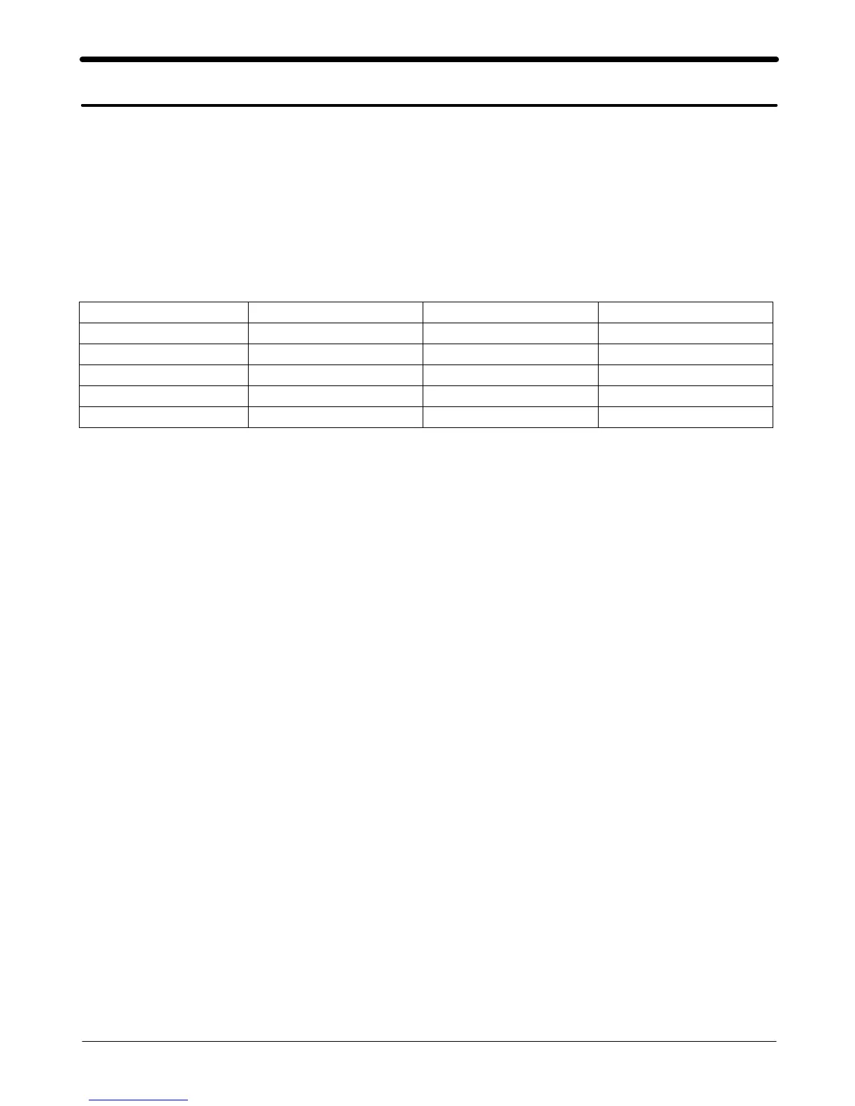
FRONT END MODULE Control Losic (MODULE1)
→
Truth Table
VC1 VC2 VC3
Tx Mode (GSM900) H L L
Tx Mode (DCS1800/1900) L H H(L)
Rx Mode (GSM900) L L L
Rx Mode (DCS1800) L L L
Rx Mode (PCS1900) L L H
—
VC-TCXO (U102)
This module generates the 26MHz reference clock to drive the logic and RF.
It is turned on when the supply voltage +VCC_SYN is applied.
After buffering a reference clock of 26MHz is supplied to the other parts of the system
through the transceiver pin OUT.
—
TRANSCEIVER (U100)
This chip is fully integrated GSM GPRS tri-band transceiver with VCO, loop filters and most of the
passive component in it.
And also fully integrated fractional N RF synthesizer with AFC control possibility, RF VCO with integrated supply
regulator. Semi integrated reference oscillator with integrated supply regulator.
RF Receiver front-end amplifies the E-GSM900, DCS1800 and PCS1900 aerial signal, convert the chosen channel
down to a low IF of 100kHz.
In IF section, further amplifies the wanted channel output level to the desired value and rejects DC.
2-1-2. TX PART
The transmitter is fully differential using a direct up conversion architecture. It consists of a signal side band
power up mixer. Gain is controlled by 6 dB via 3-wire serial bus programing. The fully integrated VCO and power
mixer achieve LO suppression, quadrature phase error, quadrature amplitude balance and low noise floor specification.
Output matching/balun components drive a standard 50 ohms single ended load.