EasyManua.ls Logo

Sangean ATS-818 Service Manual

Sangean ATS-818
71 pages
To Next Page IconTo Next Page
Page #1 background imageLoading...
Page #1 background image
Ls
ATS-818
A
World
of
Listening
SANGEAN
AS
memo)
DIGITALTUNING.
Ee
ALEAND
MW
FW/SuiW
Bro
©
|ecvaie—
arm
SUZER
|]
warreny
|]
SLEEP
@)
[AUTO
scan]
PLL
SYNTHESIZED
worLbD
BAND
RECEIVER
The
SANGEAN
ATS-818
is
the
WORLD'S
ONLY
Portable
World
Band
Receiver
offering
more
features
and
performance
than
many
expensive
table
top
Short
Wave
Receivers.
PLU45|O-|&
(CO
lOlE|@
synneseeo
RADI
inectwven
||
memory
|{
‘ocx
||
uct
||
rime
Ser
|[OUAL
Time]
[FM
STEREO]
art
*
All
SW
Bands
from
120m
to
11m
_—_*
45
Memory
Presets
*
RF
Gain
Control
*
Radio/Buzzer
Clock
Alarm
*
AM
Wide/Narrow
Filter
*
Dual
Conversion
Receiver
*
BFO
for
Single
Side
Band
&
CW
*
Dual
Time
Display
for
Local
*
Signal
Strength
&
Battery
*
Continuous
AM
Coverage
and
UTC
Time
Indicator
from
150-29999KHz
plus
FM
87.5-
*
Adjustable
Sleep
Timer
*
Tone
Control
&
Safety
Lock
108MHz
*
Five
Tuning
Methods:
Direct
frequency
Input,
Auo
Scan,
Manual
Scan,
Memory
Recall,
Rotary
Dial
SPECIFICATIONS
]
FREQUENCY
2.300-2.495MH2(120m)
3.200-3.400(90m)
3.900-4000(75m)
4.750-5.060(60m)
5.950-6200MHz(49m)
7.100-7.300(4
1m)
9.500-9.900(3
1m)
11.650-12.050(25m)
|
413.600-13.800(21m)
15.100-15.600(19m) 17.550-17.900(16m)
21.450-21.850(13m)
|
25.670-26.100(11m)
SEMI-CONDUCTORS:
1
LSI,
12
IC’s,
8
FET's,
48
Trans.,
45
Diodes.
2
LED
|
OUTPUT
PWR:
800mW
|
SPKR:
4
inch,
4
ohm
BATTERIES:
4/1.5VDC
“D”
Size
Radio Power
&
3/1.5VDC
AA
Back-Up
Power
_|
ACCESSORIES:
AC
Adapt,
Ext.
Antenna
Adapt,
Shortwave
HandBook
2651
Troy
Avenue,
South
El
Monte,
CA
91733
AMERICA,
INC.
Tel:
(818)
579-1600
Fax:
(818)
579-6806

Other manuals for Sangean ATS-818

Question and Answer IconNeed help?

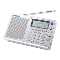
Do you have a question about the Sangean ATS-818 and is the answer not in the manual?

Sangean ATS-818 Specifications

General IconGeneral
TypePortable Radio
ModulationAM / FM
Headphone Jack3.5 mm
DisplayLCD
Tuning SystemPLL Synthesized
Frequency RangeFM: 87.5-108 MHz, MW: 522-1620 kHz, SW: 1.711-29.999 MHz
Tuning StepsFM: 50 kHz, MW: 9 kHz, SW: 5 kHz
FM Sensitivity3 μV
SW Sensitivity20 μV
IF FrequenciesFM: 10.7 MHz, AM: 455 kHz
Audio Output Power0.5 W
AntennaTelescopic antenna for FM
Power SourceAC adapter or batteries
Battery LifeUp to 20 hours
Memory Presets10 FM, 5 MW, 5 SW

Summary

Specifications

Disassembly Instructions

Block Diagram

Alignment Instructions

Alignment For Clock Time Accuracy

Adjust TC401 to set clock time accuracy.

Alignment For PLL Frequency

Adjust TC4 for PLL frequency accuracy at 108 MHz.

Alignment For AM 2nd Local OSC

Adjust L14 for AM 2nd Local OSC frequency.

Alignment For AM 2nd IF

Adjust T4 and T6 for AM 2nd IF frequency response.

Alignment For FM IF

Adjust T5 and T7 for FM IF response curve.

Alignment For AM Sensitivity

Adjust T1, T3, and L14 for AM sensitivity.

Alignment For BFO

Adjust TC3 for minimum reading on SSVM for BFO alignment.

Alignment For FM Sensitivity

Adjust L11, L12, TC1, TC2 for FM sensitivity.

Alignment For MPX

Adjust SVR2 for MPX frequency range.

Alignment For Indication Level of Battery

Adjust SVR5 to calibrate battery level indicator.

Alignment For Signal Strength Level

Adjust SVR3 and SVR4 for signal strength level readings.

Alignment For 450kHz Trap

Adjust T8 for minimum audio output in 450kHz trap alignment.

Alignment For FM Station Detection

Adjust SVR1 for FM station detection voltage difference.

Troubleshooting Flow Chart

Weak Sensitivity on FM Mode

Troubleshooting steps for weak FM sensitivity.

Weak Sensitivity in AM Band

Troubleshooting steps for weak AM band sensitivity.

PLL Does Not Work

Troubleshooting steps when the PLL circuit is not functioning.

Power Cannot Be Turned On

Troubleshooting steps when the device cannot be powered on.

Wiring Diagram

Main PCB Chip Side

Main PCB Top View

Control PCB Chip Side

Control PCB Top View

Electrical Parts List

Semiconductor Lead Identifications

Exploded View

Mechanical Parts List

IC Circuit Block Diagram

IC3-CX7961A-1

Block diagram for IC3 CX7961A-1.

IC4-TC74HC148AP

Block diagram for IC4 TC74HC148AP.

IC1-TA7758P

Block diagram for IC1 TA7758P.

IC2-AN7415

Block diagram for IC2 AN7415.

IC5,6-TA75339AP/P

Block diagram for IC5,6 TA75339AP/P.

IC7,8-AN7141N

Block diagram for IC7,8 AN7141N.

IC9-LA5003

Block diagram for IC9 LA5003.

IC401,402-S81237AG-RE-T2

Block diagram for IC401,402 S81237AG-RE-T2.

IC403-UPD75308GF-177

Block diagram for IC403 UPD75308GF-177.

ICS' & Transistors' Voltage List

Schematic Diagram

Related product manuals