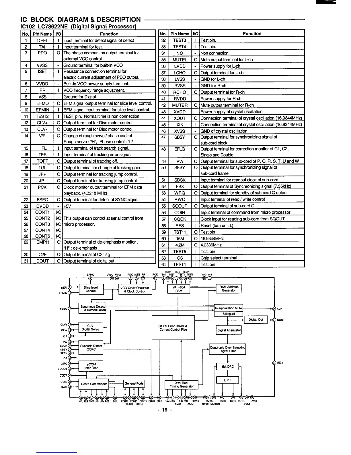
IC BLOCK DIAGRAM & DESCRIPTION
Cl 02 LC78622NE (Digital Signal Processor)
No. Pfn Name Uo
Function
1 DEFI I input terminal for detect signai of defect
2 TAi I input terminal for test.
3
PDO
o The phase comparison output terrninai for
extemai VCO control.
4 Vvss - Ground terminai for built-in VCO
5
ISET I Resistance connection terminal for
eiectric current adjustment of PDO output.
6
VVDD - Built-in VCO power supply terminal.
7 FR I VCO frequency range adjustment.
8
Vss
- Ground for Digital
9 EFMO o EFM signal output terminal for slice level control.
10 EFMIN I EFM signai input terminai for slice ievel control.
11 TEST2
I
TEST pin. Normai time is non connection.
12
CLV+ o Output terminai for Disc motor controi.
13 CLV- 0 Output terminal for Disc motor control.
14 VIP o Change of rough servo I phase control
Rough servo: “H”, Phase control: “L”
15 HFL
i input terminai of track search signai.
16 TES I Input terminal of tracking error signal.
17 TOFF
o Output terminal of tracking off.
18 TGL o Output terminal for change of tracking gain.
19
JP+ o Output terminal for tracking jump controi.
a JP- 0 Output terminal for tracking jump controi.
21 PCK
o Cicck monitor output terminal for EFM data
piayback. (4.3218 MHz)
22 FSEQ o Output terminal for detect of SYNC signal.
23
DVDD - +5V
24 CONT1 I/o
25 CONT2 I/o This output can controi at serial control from
26 CONT3 I/o micro processor.
27 CONT4 iio
26 CONT5 ilo
29 EMPH o Output terminal of d~emphasis monitor.
“H”: de-emphasis
30 C2F
o Output terminal of C2 flag
31 DOUT o Output terminal of digital out
EFMO woo Wss
TST11TEST2 TEsT4
PDO ISET FR
PCK TAI TEST1 TESTSTESTS
Vrm Vss
VCCI Cbck Oscillator
RAM Address
t
FSEQ
Syrwmous Oetect
EFM Demodulaln
1’
I
II
CLV-
Subcode Dxrast
(??$
WRO
HFLTESTcfF JP. JP+~ TGL CC+JT~~~WNT5 El
Cl C2 Error Detec4&
Cared Control F!ag
c=’
1
DgWl Attenuator
Ml%l
)=_ ______xToD
W EFLG 16M42M FSXXIN
‘R&- R% L~O w-i’L – =DD
XV2S XOL.JT
RVSS MUTER
LVSS
C2F
(F.C)
-19-