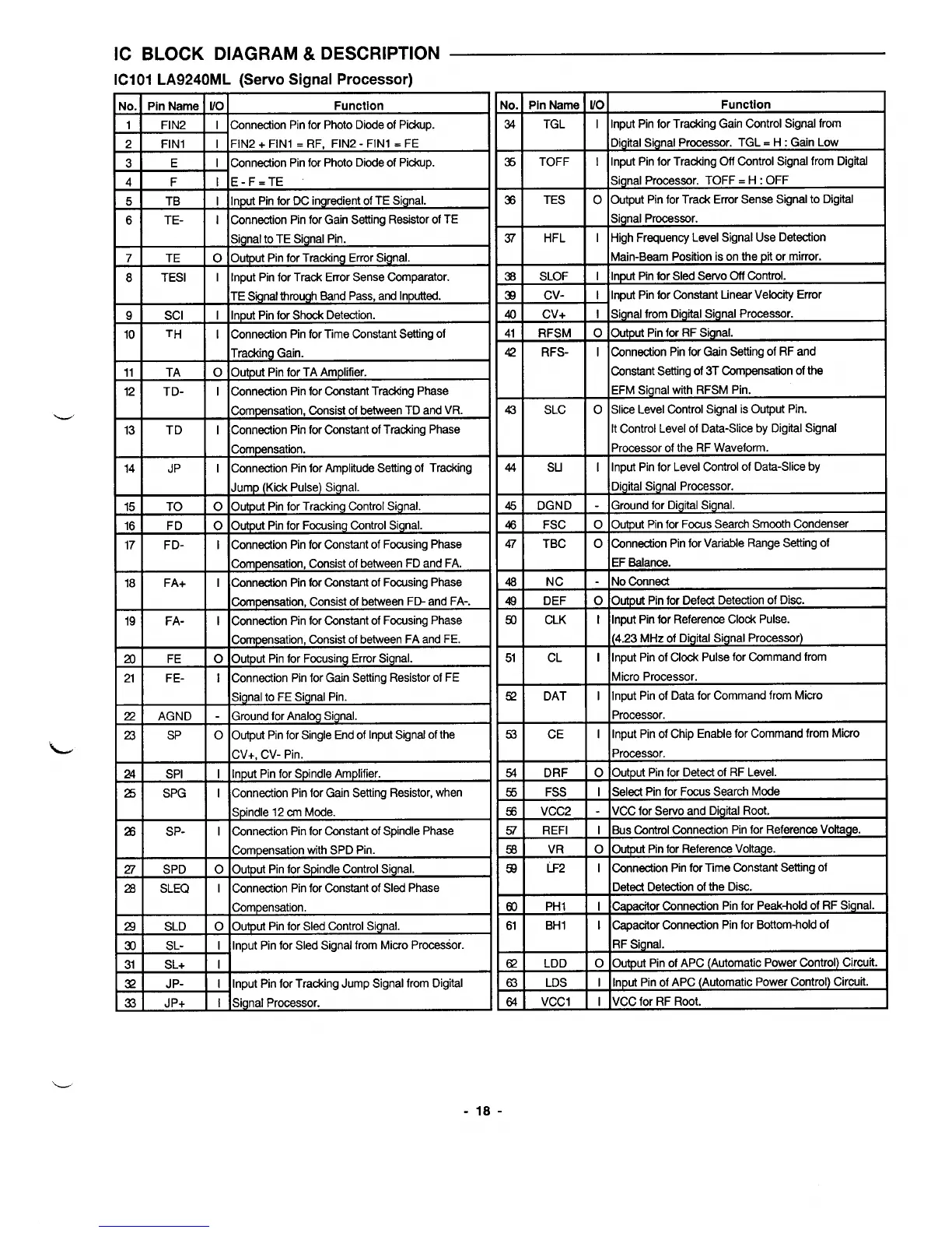
IC BLOCK DIAGRAM& DESCRIPTION
ICI 01 LA9240ML (Servo Signal Processor)
Uo. Pin Name I/o
Function
1 FIN2 I Connection Pin for Photo Diode of Pickup.
2 FIN1 I FIN2 + FIN1 = RF, FIN2- FIN1 = FE
3
E I Connection Pin for Photo Diode of Pickup.
4 F I E- F=TE
5
TB I Input Pin for DC ingredient of TE Signal.
6
TE- 1 Connection Pin for Gain Setting Resistor of TE
Signal to TE Signal Pin.
7 TE
o Output Pin for Tracking Error Signal.
8
TESI
I Input Pin for Track Error Sense Comparator.
TE Sinai through Band Pass, and Inputted.
9 Scl
I Input Pin for Shock Detection.
10 TH
I Connection Pin for Time Constant Setting of
Tracking Gain.
11 TA o Output Pin for TA Amplifier.
12 TD- 1 Connection Pin for Constant Tracking Phase
Compensation, Consist of between TD and VR.
13 TD
I Connection Pin for Constant of Tracking Phase
Compensation.
14 JP
I Connection Pin for Amplitude Setting of Tracking
Jump (Kick Pulse) Signal.
15 TO
o Output Pin for Tracking Control Signal.
16 FD
o Output Pin for Focusing Control Signal.
17 FD-
1 Connection Pin for Constant of Focusing Phase
Compensation, Consist of between FD and FA.
18
FA+ I Connectbn Pin for Constant of Faxing Phase
Compensation, Consist of between FD- and FA-.
19 FA- 1 Connection Pin for Constant of Focusing Phase
Compensation, Consist of between FA and FE.
al
FE
o Output Pin for Focusing Error Signal.
21 FE- 1 Connection Pin for Gain Setting Resistor of FE
Signal to FE Signal Pin.
z? AGND - Ground for Analcg Signal.
23
SP o Output Pin for Single End of Input Signal of the
CV+, CV- Pin.
24
SPI
I Input Pin for Spindle Amplifier.
25 SPG I Connection Pin for Gain Setting Resistor, when
Spindle 12 cm Mode.
23 sP-
1 Connection Pin for Constant of Spindle Phase
Compensation with SPD Pin.
27 SPD
o Output Pin for SpindleControlSignal.
28 SLEQ
I ConnectionPin
for Constant of Sled Phase
Compensation.
29 SLD
o Output Pin for Sled Control Signal.
33 SL-
1 Input Pin for Sled Signal from Micro Processor.
31 SL+ I
32
JP- 1 Input Pin for Tracking Jump Signal from Digital
33 JP+
I Signal Processor.
-18-