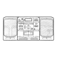
- 22 -
IC BLOCK DIAGRAM & DESCRIPTION
IC818 SST39VF800A-70-4C-EK(Flash Memory)
IC850 PQ2L2182MS(regulater)
Memory Address
Address Buffer
& Latches
Control Logic
X-Decoder
SuperFlash
Memory
Y-Decoder
I/O Buffer and Data
Latches
DQ
15
-DQ
0
CE#
OE#
WE#
Symbol
Pin Name
Function
To provide memory addresses. During Sector-Erase AMS-A11 address
lines will select the sector. During Block-Erase A
MS-A15 address lines will
select the block.
To output data during Read Cycles and receive input data during Write
Cycles.
Data is internally latched during a Write Cycle.
The outputs are in tri-state when OE# or CE# is high.
To activate the device when CE# is low.
To gate the data output buffers.
To control the Write operations.
To provide power supply voltage:
Unconnected pins
3.0-3.6V for SST39LF200A/400A/800A
2.7-3.6V for SST39LF200A/400A/800A
Address Inputs
Data Input/output
Chip Enable
Output Enable
Write Enable
Power Supply
Ground
No connection
AMS
1-A0
DQ15-DQ0
CE#
OE#
WE#
V
DD
VSS
NC
3
15
4
2
CONTROL
IC851 PQ070XZ01Z(Regulater)
1
Description
DC INPUT
ON/OFF CONTROL
DC OUTPUT
OUTPUT VOLTAGE ADJUSTMENT
GND
1
2
3
4
5
Symbols
Vin
Vc
Vo
Vadj
2 3 4 5
Pin No.
IC852 PQ1X501M2Z(Regulater)
15
34
2
CONTROL
DC output : VoDC input : Vin
ON/OFF control : Vc
GND
Noise reduction : Nr
 Loading...