,.. ,
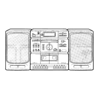
IC BLOCK DIAGRAM (CD)
ICI04 LC7866E (Digital Signal Processor)
.
..”
DESCRIPTION
1 TFST1
I
I
For TEST. Ntirmal lime !S non connection.
2
AO
o
Input from vCO output ,n LA921O .(8.6436 MHz)
3
Al 1
Phase comparbon OUIPU1
of VCO and EFM signal.
4
PDO
o
6
I
FRO
I
o
7 EFMO
o
8
EFMIN
I
9
TEST2 1
10
CLV +
o
11
CLV-
0
12
VIP 0
13 FOCS 0
14
FST
0
—
15
FZO I
16
HFL I
17
TES 1
4--
19 I FSEQ
-1-
20
TOFF
21
TGL
+=
22
THLO
23
TEST3
k
0
0
0
0
0
.1
~
Z5
JP + o
26
JF’”0
27
oEMO I
28
TEsT4- I
29 EMPH
0
30
TESTA
EFMIN
FSEC
CLV+
CLV-
v/P
PH SBCK
SL3SY SFSY
URO SOOUT
M/L
COCK
Colh
Rwc
DEMC
Neaative outwt throuqh amdnude hmiter. Anlighase of
-.
EFMO. This signal use SLICE LEVEL CONTROL.
Positive output through ampl)tude Iimller. Ant,phase of EFMO.
This signal use S1 ICE LEVEL CONTROL.
Inputting HF signal of l-2Vp.P This s,gnal use SLICE LEVEL
CONTROL.
For TEST. Normal time is non connection.
Oulput for OISC MOTOR CONTROL.
Output for DISC MOTOR CONTROL.
CLV rough Servo time : Output “H-.
Phase control Ome : Output”L.
Output ‘H- : Lens pull UP wnh slowly than stop the Focus
—
Servo. If FZO generale, Et reset output of FOCS.. For Iead.in of
Focus
Comply with command of track jump, 11 oscillate kick Pulse.
JP + & JP”. It jump the prescribed number of track (1.4, ?6,64)
Comply with command of track jump. it osc,llate kick Pulse.
JP + & JP_. It jump the prescribed number of track (1,4,16,64).
PCK Monitor (4.3218MHz)
SYNC (FS of truth) detected from EFM signal = SYNC of
counter :
‘H- (Latch Oulput during in 1 frame)
Comply with command of track jump, it oxillate kick Pulse,
JP + & ,P-. ,t jump the prescribed number of track (1,4716.64).
For TEST. Normal time is non connection.
+ 5V
Comply with command of track jump, it oscillate kick Pu!se,
JP + & JP-.
Itjump the pre$crlbed number of track (1 ,4.16,64).
For adjustment of production process. Sound on function,
For TEST. Normal time is non connection.
Output is “H- time, !t need de-emphas, s
Fc,r TEST. Normal t,me is H..
No
PIN
1/0
NAME
31
srJF’2 o
32 SMP1
o
33
LF(CLK
o
34
srfl P
o
35
oFOUT o
36
DACLK o
37
TES7B
o
38
TESTC
o
39 CK2
o
40
ROM OUT o
41
C2FLCK o
42 C2F
o
43
O(JUT o
44
SBSY o
45
EFLG o
46
Pw o
47
SFSY o
48
SBCK
I
49
FSX
o
50
WF(Q 0
51 Rwc
I
52 SCJOUT o
53 COIN
I
54 —
CQCK
i
55
RES
I
56
M/L
I
57 LASER
o
58
1614
0
59
4M o
60 CONT
o
61
TESTS
I
62 Cs
I
63
XIN
1
64
xt)uT o
SYFWZHRONIZATION
EFM OEMOOULATION
INTERPOLATION
MUTE
1
1 r
,
I
.JCOM
INTERFACE
SERVO
COMMANOER
.,4110
E $’l:i~
wlrl.~
g=73
>
DESCRIPTION
Oulput of wgnal to DAC, Signal of Latch & L/R select. $gnal
for Sarnplhng Hold
Output of $ignal to OAC. Signal of Latch & L / R select. S!gnal
for Sampling Hold
Output Of signal to DAC. S,gnal of Latch & L/R $elect, S!gnai
for Sampling Hold
Output of si$nal 10 OAC. Signal of Latch S L/R select. S19na’
for Sampling Hold
For TEST. Normal time ,S non connecl! on.
For TEST Normal time ,s non connection.
For output of signal that Comply w!th CO. ROM
For output of signal that Comply with CO.RO14
For output of s,onal that Con-ply w]lh CD. ROM
For output of signal that Comply with CO-ROM
Output of OIGITAL OUT
Synchronizing signal of sub-code block.
For correction monitor of Ct, c2, $ingle, double,
SFSY is Synchronizing signal of sub.code & frame. Clock of
eighth send to SBCK then read out the sub.code of P, 0, R, S
T, U, V, & W,
Output of Synchronizing signal (7.35KHz)
Oata sub.code Q pass the CRC check then WRQ do “H-. It
cetect at external, Oata read out from SC20UT by send the
CL2CK. RWC set the “H. by Micro Proce%or t!>en il let
command by $end w$th Synchronizing CQCK command data.
Turn on the Power Supply time : Once ‘L-
Oata of SQOUT want at the LRS first time : M /L set the “L-
This output can control at Serial Control from Micro Proce$$w,
16M Output (16.9344 M!!:)
4M output (4.2336MHz)
This output can control at Serial Control from Micro l’roc?sw
For TEST. Normal time is non connection.
Chip select Terminal. This terminal ‘L- : LC7866 is active
(Internal Resi>lor : Pull Down)
Connect(on Terminal of crystal oscillation (16.9344MHz)
Connectmn Terminal of crystal oscillation (16.9344MHz)
:2FCLK
:RSY
:2F
?OMOUT
)OUT
-22-