EasyManua.ls Logo

Sanyo DC-F320 User Manual

Sanyo DC-F320
56 pages
To Next Page IconTo Next Page
Page #1 background imageLoading...
Page #1 background image
Service Manual
FILE NO.
Mini Component System
DC-F320
(UK)
(W
CONTENTS
SPECIFICATION......................................................................
1
WHAT TO DO IF.......................................................................
1
LASERBEAMSAFETYPRECAUTIONS
................................
2
REMOVAL
&
INSTALLATION
.................................................
2
TUNERADJUSTMENT
............................................................
4
CDCHANGER
OPERATION
DESCRIPTION..........................
5
CD
CHANGERREPLACEMENT
.............................................
7
CD
MECHANISMADJUSTMENT
............................................
9
CD PLAYER ADJUSTMENTS
...............................................
11
TAPEDECKADJUSTMENTS
...............................................
13
EXPLODED
VIEW(CABINET
&1
CHASSIS)
..........................
15
r_:-_------__-__-____-_~
I
This serwce manual consists of “DGF320U (Main unit),
I
“RB-F320”(Remote control) and “SX-F320RUXE
,
I
LSX-F321
R,UUK”(FrontSpeaker system)
.
I
-_----------B----w
J
WEI
PRODUCT CODE No.
129 547
Ol(UK)
129 547 02(XE)
PARTSLIST
. . . . . . . . . . . . . . . . . . . . . . . . . . . . . . . . . . . . . . . . . . . . . . . . . . . . . . . . . . . . . . . . . . . . . . . . . . .
17
EXPLODEDVIEW
(TAPEMECHANISM)
. . . . . . . . . . . . . . . . . . . . . . . . . . . . . .
23
EXPLODED VIEW (CD CHANGER
&
BASE MECHANISM). 24
EXPLODED VIEW (CD CHANGER MECHANISM)
.,.a,....,.....
25
IC
BLOCKDIAGRAM
&
DESCRIPTION
. . . . . . . . . . . . . . . . . . . . . . . . . . . . . . .
28
IC
&
TRANSISTOR
VOLTAGES . . . . . . . . . . . . . . . . . . ..a.......................
34
WIRINGCONNECTION
. . . . . . . . . . . . . . . . . . . . . . . . . . . . . . . . . . . . . . . . . . . . . . . . . . . . . . . . . .
36
SCHEMATICDIAGRAM
. . . . . . . . . . . . . . . . . . . . . . . . . . . . . . . . . . . . . . . . . . . . . . . . . . . . . . . . .
37
WIRINGDIAGRAM
. . . . . . . . . . . . . . . . . . . . . . . . . . . . . . . . . . . . . . . . . . . . . . . . . . . . . . . . . . . . . . . . .
47
CABLECONNECTION
. . . . . . . . . . . . . . . . . . . . . . . . . . . . . . . . . . . . . . . . . . . . . . . . . . . . . . . . . . .
55
REFERENCE No.
SM580903
All manuals and user guides at all-guides.com
all-guides.com
Question and Answer IconNeed help?

Do you have a question about the Sanyo DC-F320 and is the answer not in the manual?

Sanyo DC-F320 Specifications

General IconGeneral
BrandSanyo
ModelDC-F320
CategoryStereo System
LanguageEnglish

Summary

Specifications and Troubleshooting Guide

What to Do If Unit Malfunctions

Laser Beam Safety Precautions

Removal and Installation Procedures

Tuner Adjustment Procedures

CD Changer Operation Description

CD Changer Replacement Guide

CD Changer Component Setup

CD Mechanism Adjustments and Maintenance

CD Mechanism Component Replacement

CD Player Adjustment Procedures

CD Pick-up Lens Maintenance

CD Player Tracking Balance and Eye Pattern Adjustments

Tape Deck Adjustment Procedures

Product Parts List

Product Safety Notice

Important safety precautions to be followed during servicing.

Component Parts Lists

Fixing Parts Identification

Printed Circuit Board Parts Lists

Additional PCB Parts Lists

Deck PCB Parts Identification

Tape Mechanism Parts List

CD Mechanism Parts Identification (Part 1)

CD Mechanism Parts Identification (Part 2)

Integrated Circuit Block Diagrams and Descriptions

IC101 CXA1782CQ (Servo Signal Processor)

Block diagram and pin function description for IC101.

IC231 LA1 832ML

Block diagram and pin function description for IC231.

Integrated Circuit Block Diagrams (Continued)

IC102 BA6398FP (Power Driver)

Block diagram and pin function description for IC102.

IC104 CXD2508AQ (Digital Signal Processor)

Block diagram and pin function description for IC104.

IC104 CXD2508AQ (Digital Signal Processor) Details

Detailed pin connections and functional blocks for IC104.

IC131 LB1648L

Block diagram and pin function description for IC131.

IC245 LC72131MD

Block diagram and pin function description for IC245.

IC361 BU2090F

Block diagram and pin function description for IC361.

IC371 M51167AFP

Block diagram and pin function description for IC371.

IC450 BU4052BCF

Block diagram and pin function description for IC450.

IC458 BH3854AFS

Block diagram and pin function description for IC458.

IC132 LB1641L

Block diagram and pin function description for IC132.

IC372 BA3126N/UPC1330HA

Block diagram and pin function description for IC372.

IC602 BA3835S

Block diagram and pin function description for IC602.

Integrated Circuit Pin Descriptions

C601 M38197MAA-613FP Pin Details

Pin, terminal, and port descriptions for the M38197MAA-613FP IC.

LA6458D/NJM4558 IC Pin Descriptions

Pin descriptions for LA6458D/NJM4558 ICs.

TC4011 BF IC Pin Descriptions

Pin descriptions for the TC4011 BF IC.

IC and Transistor Voltage Measurements

IC101 CXA1782BQ Voltage Table

Voltage table for IC101 (CXA1782BQ) under different operating modes.

IC102 BA6398FP Voltage Table

Voltage table for IC102 (BA6398FP) under different operating modes.

IC104 CXD2508AQ Voltage Table

Voltage table for IC104 (CXD2508AQ) under different operating modes.

IC106 NJM4558D Voltage Table

Voltage table for IC106 (NJM4558D) under different operating modes.

IC131 LB1648 Voltage Table

Voltage table for IC131 (LB1648) under different operating modes.

IC and Transistor Voltage Measurements (Continued)

IC132 LB1641 Voltage Table

Voltage table for IC132 (LB1641) under different operating modes.

IC601 M38198MC-613FP Voltage Table

Voltage table for IC601 (M38198MC-613FP) under different operating modes.

IC602 BA3835S Voltage Table

Voltage table for IC602 (BA3835S) under different operating modes.

Transistor Voltage Tables

Voltage tables for various transistors.
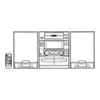
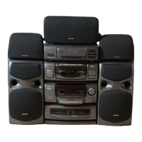
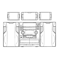
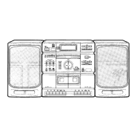
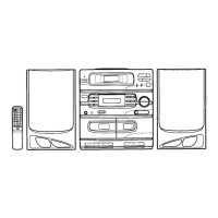
Wiring Connection Diagram

CD Section Schematic Diagram

CD Schematic Diagram Details

Tape Deck Section Schematic Diagram

Tape Deck Schematic Diagram Details

Front Panel Section Schematic Diagram

Front Panel Schematic Diagram Details

Amplifier Section Schematic Diagram

Amplifier DC Voltage Conditions

Tuner Section Schematic Diagram

Tuner Schematic Diagram Details

CD Section Wiring Diagram

Sub-Assembly Wiring Diagrams

Tape Deck Section Wiring Diagram

Tape Deck Wiring Diagram Details

Front Panel Section Wiring Diagram

Front Panel Wiring Diagram Details

Amplifier and Tuner Wiring Diagram

Amplifier and Tuner Wiring Diagram Details

Cable Connection Guide

Related product manuals