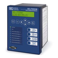
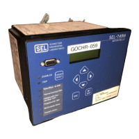
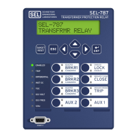
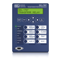
Date Code 20170814 Instruction Manual SEL-700G Relay
List of Tables
Inst ruction Manual
Table 1.1 Current (ACI) and Voltage (AVI) Card Selection for SEL-700G Models ............................. 1.2
Table 1.2 Protection Elements in SEL-700G Models............................................................................ 1.2
Table 1.3 Recommended Protection Elements by Generator Grounding Method.................................1.4
Table 1.4 SEL-700G Serial Port Settings............................................................................................... 1.9
Table 2.1 Power Supply Inputs (PSIO/2 DI/3 DO) Card Terminal Designations..................................2.4
Table 2.2 Communications Ports ........................................................................................................... 2.4
Table 2.3 Communications Card Interfaces and Connectors................................................................. 2.5
Table 2.4 Current/Voltage Inputs (3 ACI/4 AVI) Card Terminal Designations .....................................2.6
Table 2.5 Current/Voltage Inputs (3 ACI/2 AVI) Card Terminal Designations .....................................2.7
Table 2.6 Currents Inputs (3 ACIE) Card Terminal Designations......................................................... 2.7
Table 2.7 Voltage Inputs (2 AVI) Card Terminal Designations ............................................................. 2.8
Table 2.8 Current/Voltage Inputs (4 ACI/3 AVI) Card Terminal Designations .....................................2.8
Table 2.9 Current Inputs (3 ACIZ) Card Terminal Designations........................................................... 2.9
Table 2.10 Current Input (1 ACI) Card Terminal Designation ................................................................2.9
Table 2.11 Four Analog Inputs/Four Analog Outputs (4 AI/4 AO) Card Terminal Designations......... 2.10
Table 2.12 I/O (3 DI/4 DO/1 AO) Card Terminal Designations............................................................ 2.10
Table 2.13 RTD (10 RTD) Card Terminal Designations........................................................................ 2.11
Table 2.14 Four Digital Inputs/Four Digital Outputs (4 DI/4 DO) Card Terminal Designations.......... 2.11
Table 2.15 Eight Digital Inputs (8 DI) Card Terminal Designations.....................................................2.12
Table 2.16 Eight Digital Outputs (8 DO) Card Terminal Designations................................................. 2.12
Table 2.17 Four Digital Inputs, One Form B Digital Output, Two Form C Digital Outputs
(4 DI/3 DO) Card Terminal Designations ........................................................................ 2.13
Table 2.18 Jumper Functions and Default Positions.............................................................................. 2.18
Table 2.19 Typical Maximum RTD Lead Length ..................................................................................2.22
Table 3.1 SEL Software Solutions ......................................................................................................... 3.1
Table 3.2
ACSELERATOR QuickSet SEL-5030 Software.......................................................................3.1
Table 3.3 File/Tools Menus....................................................................................................................3.7
Table 3.4 QuickSet Help ...................................................................................................................... 3.15
Table 4.1 Identifier Settings ................................................................................................................... 4.3
Table 4.2 Configuration Settings............................................................................................................4.4
Table 4.3 Differential Element Settings............................................................................................... 4.12
Table 4.4 Ground Differential Settings ................................................................................................ 4.33
Table 4.5 Restricted Earth Fault Settings.............................................................................................4.36
Table 4.6 Stator Ground Protection Settings........................................................................................ 4.40
Table 4.7 Field Ground Protection Settings......................................................................................... 4.47
Table 4.8 Compensator Distance Protection Settings .......................................................................... 4.48
Table 4.9 Voltage Controlled/Restraint Time OC Protection Settings.................................................4.52
Table 4.10 Loss-of-Field Protection Settings......................................................................................... 4.57
Table 4.11 Current Unbalance Settings..................................................................................................4.61
Table 4.12 Thermal Overload Settings................................................................................................... 4.65
Table 4.13 Volts-Per-Hertz Settings.......................................................................................................4.69
Table 4.14 Frequency Accumulation Settings ....................................................................................... 4.74
Table 4.15 Out-of-Step Protection Settings ...........................................................................................4.77
Table 4.16 Inadvertent Energization Protection Settings....................................................................... 4.86
Table 4.17 Phase Overcurrent Settings ..................................................................................................4.87
Table 4.18 Neutral Overcurrent Settings................................................................................................4.88
Table 4.19 Residual Overcurrent Settings.............................................................................................. 4.93
Table 4.20 Negative-Sequence Overcurrent Settings............................................................................. 4.93
Table 4.21 Maximum Phase Time-Overcurrent Settings....................................................................... 4.94
Table 4.22 Negative-Sequence Time-Overcurrent Settings................................................................... 4.95
Table 4.23 Neutral Time-Overcurrent Settings......................................................................................4.96
Table 4.24 Residual Time-Overcurrent Settings....................................................................................4.96
Table 4.25 Equations Associated With U.S. Curves.............................................................................. 4.98



 To Next Page