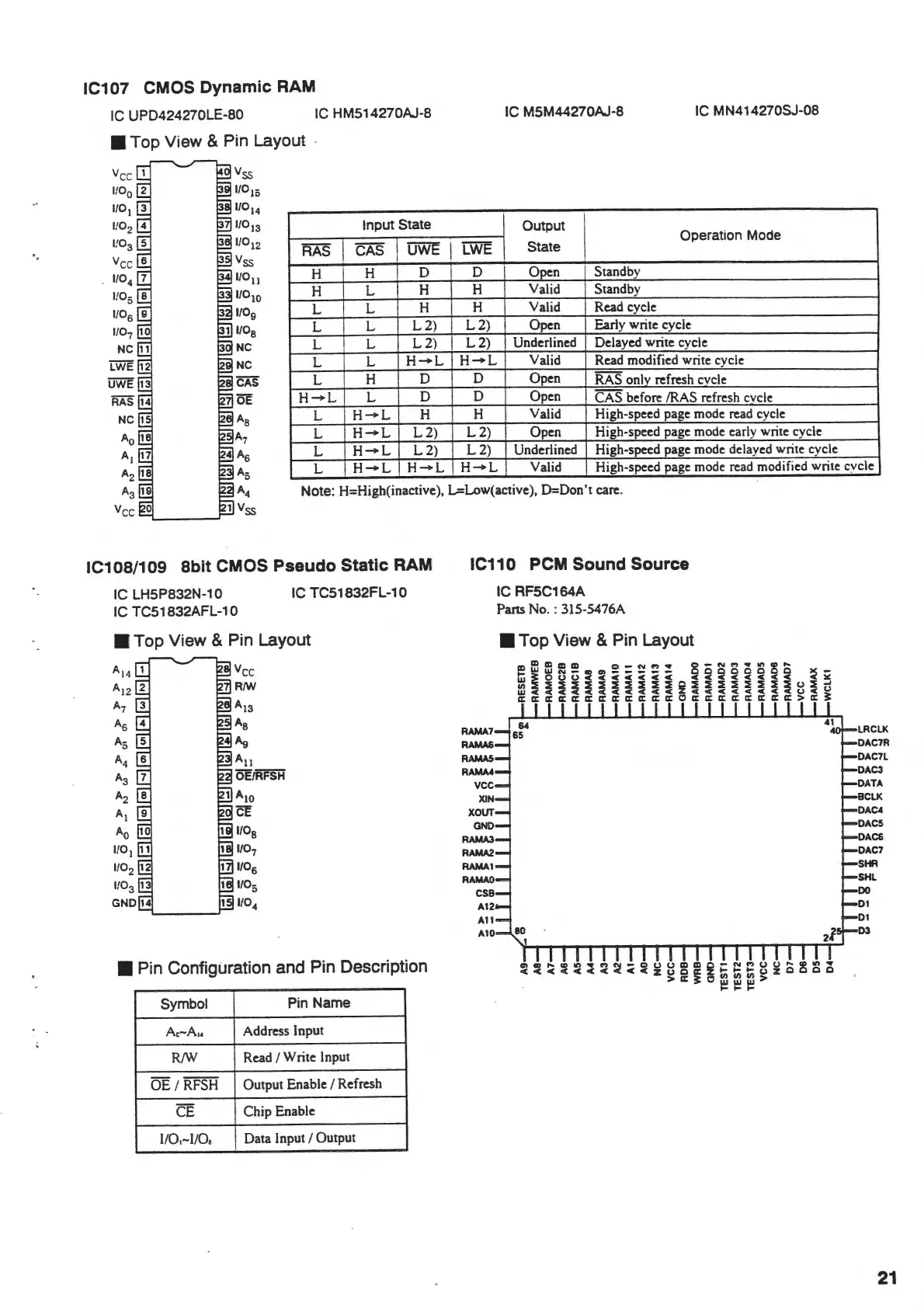
IC107 CMOS
Dynamic
RAM
IC
UPD424270LE-80
IC
HM514270AJ-8
IC
M5M44270AJ-8
IC
MN414270SJ-08
•Top
View & Pin Layout
Vss
11015
11014
11013
11012
Vss
11011
Input
State
Output
Operation
Mode
RAS
CAS
I UWE
I
LWE
State
I
H
H
D D
I
Ooen Standby
11010
H
L
H
H
Valid Standby
1109
L
L
H
H
Valid Read cycle
L
L
L 2)
L2)
Open Early write cycle
NC
L
L
L2)
I
L2)
Underlined Delayed write cycle
NC
L
L
H-+L H-+L
Valid
Read modified write cycle
'CAS
L
H
D D
Open
RAS onlv refresh cvcle
i5E
H-+L
L
D D
Open
CAS before /RAS refresh cvcle
As
L
H-+L
H
H
Valid
High-speed page mode read cycle
A1
L
H-+L
L2) L2)
Open
High-speed page mode early write cycle
L
H-+L
L2)
L2)
Underlined High-speed page mode delayed write cycle
A5
L
H-+L
H-+L
H-+L
Valid High-speed page mode read modified write cvcle
A4
Note: H=High(inactive), L=Low(active), D=Don't care.
1 Vss
IC108/109 Sblt CMOS
Pseudo
Static
RAM
IC
LH5P832N-10
IC
TC51832AFL-10
IC
TC51832FL-10
•Top
View & Pin Layout
Vee
RfW
A13
As
Ag
Au
OE/RFSH
1 A
10
CE
• Pin Configuration and Pin Description
Symbol
Pin
Name
A,-A,.
Address Input
R/W
Read
I Write Input
OE/
RFSH
Output Enable
I Refresh
CE
Chip Enable
1/0,-1/0,
Data Input I Output
IC11 O PCM
Sound
Source
IC
RF5C164A
Parts
No. : 315-5476A
•Top
View & Pin Layout
21