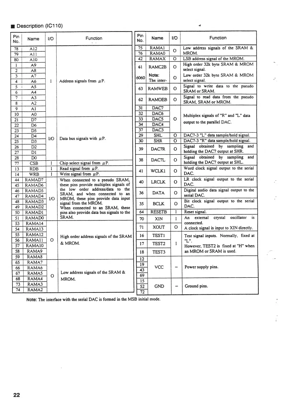
• Description (IC110)
Pin I
Name
,,0
I
Function
No.
1
Pin
Name
1/0
Function
No.
78
Al2
79
All
75
RAMAi
0
Low address signals
of
the SRAM &
76
RA
MAO
MROM.
80 AlO
42
RA
MAX
0
LSB address signal
of
the MROM.
1 A9
2
A8
(i
I
RAMC2B
0
High order 32k byte SRAM & MROM
select signal.
3
A7
4 A6
I
Address signals from µ.P.
6060
Note:
0
Low order 32k byte SRAM & MROM
The inter-
select signal.
5
i
AS
6
I
A4
63
RAMWEB
0
Signal to write data to the
pseudo
SRAM
or
SRAM.
7
I
A3
8 A2
62
RAMO EB
0
Signal to read data from the
pseudo
SRAM, SRAM
or
MROM.
9
Al
31
DAC7
10
AO
21
D7
22
D6
32 DAC6
Multiplex signals
of
"R" and "L" data
33
DAC5
0
34
DAC4
output to the parallel DAC.
23
DS
37
DAC3
24
D4
l!O
Data bus signals with µ.P.
25
D3
29
SHL
0
DAC7-3 "L" data sample/hold signal.
30
SHR
0
DAC7-3 "R" data sample/hold signal.
26
D2
27
DI
39
DAC7R
0
Signal
obtained
by
sampling
and
holding the DAC7 output at SHR.
28
DO
77
CSB
I
Chip select signal from
µ.
P.
38
DAC7L
0
Signal
obtained
by
sampling and
holding the DAC7 output at SHL.
13
RDB
I
Read signal from
µ.P.
14
WRB
I
Write signal from µ.P.
41
WCLKl
0
Word clock signal output to the serial
DAC.
44
RAMAD7
When connected to a pseudo SRAM,
45
RAMAD6
these pins provide multiplex signals
of
40 LRCLK
0
LR clock signal output to the serial
DAC.
46
RA
MADS
the low order address/data to the
47
RAMAD4
SRAM, and when connected to an
48
RAMAD3
110
MROM, these pins provide data input
signal from the MROM.
49 RAMAD2
When connected to an SRAM, these
36
DATA
0
Digital audio data signal output
to
the
serial DAC.
35 BCLK
0
Bit clock signal output to the serial
DAC.
50
RAMADI
pins also provide data bus signals to the
64
RESETB
I
Reset signal.
51
RAMA
DO
SRAM.
70
XJN
I
An
external crystal
oscillator IS
53
RAMAl4 connected.
54
RAMAl3
71
XOUT
0
A clock signal is input to XIN directly.
55
RAMA12
High order address signals
of
the SRAM
56
RAMAi!
0
57 RAMAIO
&MROM
.
16 TEST!
Test signal inputs. Normally, fixed at
17
TEST2 I
"L".
However, TEST2
is
fixed at "H" when
58
RAMA9
18
TEST3
an
MROM
or
SRAM
is
used.
59 RAMA8
65
RAMA7
66
RAMA6
67 RAMA5
0
Low address signals
of
the SRAM &
68 RAMA4
MROM.
73
RAMA3
74
RAMA2
12
-
19
vcc
Power supply pins.
-
-
43
-
69
15
-
GND
Ground pins.
52
-
>-----
72
Note: The interface with the serial DAC
is
formed in the MSB initial mode.
22