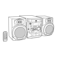
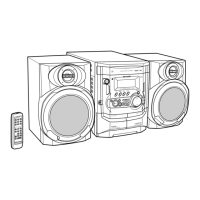
CD-XP700/CD-XP7700
– 50 –
IC3 VHiLC78683E-1: MP3 Decoder (LC78683E) (2/2)
51 DVDD4 Input I/O digital supply pin.
52 VSS — GND ground pin.
53 MADRS7 Output DRAM address output 7.
54 MADRS6 Output DRAM address output 6.
55 MADRS5 Output DRAM address output 5.
56 MADRS4 Output DRAM address output 4.
57 MADRS3 Output DRAM address output 3.
58 MADRS2 Output DRAM address output 2.
59 MADRS1 Output DRAM address output 1.
60 MADRS0 Output DRAM address output 0.
61 DVDD5 Input Internal logic supply pin.
62 VSS — GND ground pin.
63* STREQ Input/Output MP3 data demand flag output. (H-active)/DRAM data demand flag input. (H-active)
64* STCK Input/Output MP3 data transfer clock input./DRAM data transfer clock output.
65* STDAT Input/Output MP3 data serial input./DRAM data serial output.
66 FSYNC Output MP3 frame synchronization signal. (H-active)
67* CRCF Output CDROM-CRC flag output. (H-active)/DRAM data output enable signal output. (H-active)
68 DVDD6 Input I/O digital supply pin.
69 VSS — GND ground pin.
70* WOK Input DRAM write permit input. (CD-DA, H-active)/DRAM data demand flag input.
(CDROM, H-active)
71* CNTOK Output Data connection point detection completion flag. (CD-DA, H-active)/DRAM data serial
output. (CDROM, H-active)
72* OVF Output DRAM write interrupt flag. (CD-DA, H-active)/DRAM data transfer clock output.
(CDROM, H-active)
73 CMDOUT Output Command serial data output. (Nch open drain output pin)
74 CMDIN Input Command serial data input.
75 CL Input Command serial clock input.
76 CE Input Command enable input. (H-active)
77 INTB Output Interrupt signal output. (L-active)
78 RESB Input System reset. (L-active)
79 DATAIN Input CD serial data input.
80 DATACK Input CD bit clock input.
Terminal NamePin No. Input/Output
Function
In this unit, the terminal with asterisk mark (*) is (open) terminal which is not connected to the outside.
*1: Unused port
Unused input pin must always be connected to GND (0 V).
Unused output pin must be left open.
Unused I/O pin must either be connected to GND (0 V) or set to the output and left open.
*2: Be sure to supply the same potential to DVDD1, DVDD3, DVDD4, DVDD6 and AVDD.
Power supply to DVDD2 and DVDD5 must always be lower than that for DVDD1.
*3: Be sure to connect input pins TEST1 and TEST2 to GND (0 V).
*4: I/O pins (MDATA0 to 15, STREQ, STCK, STDAT) are in the input mode during initialization.
*5: At power ON, be sure to set the RESB pin to "L" (1 µs or more).
*6: It is necessary to supply to the CKIN pin the 16.9344 MHz clock from LSI for CD-DSP.
The oscillator circuit cannot be made up from this LSI and oscillator only.